Display device

a display device and display technology, applied in the field of display devices, can solve the problems of low curved region, unpractical, etc., and achieve the effect of reducing the degree of freedom in design and low degree of freedom

Active Publication Date: 2019-10-01
JAPAN DISPLAY INC
View PDF10 Cites 0 Cited by
  • Summary
  • Abstract
  • Description
  • Claims
  • Application Information

AI Technical Summary

Benefits of technology

[0006]However, the conventional configuration described above has a low degree of freedom in designing the width of the curved region in the left edge region and the right edge region of the organic light-emitting diode structure layer, that is, in a second edge-side region and a third edge-side region that cross a first edge side at which the organic light-emitting diode structure layer is connected with a film such as a COF. In the conventional configuration described above, a plurality of wiring lines are disposed on the film. The wiring lines are disposed bypassing the arrangement region of the integrated circuit mounted on the film. Therefore, the horizontal width of the film needs to be widely formed according to a wiring-line forming region disposed bypassing the arrangement region of the integrated circuit. When the horizontal width of the film becomes wide, a connection section to the film on the first edge-side region of the image display region is widened. As described above, the film is folded back onto the rear surface side. Therefore, when it is intended to curve the second and third edge-side regions in the image display region so as to include the film, bending occurs in two directions in the film, and thus this is not practical because a large stress is applied to the film. Therefore, the width of the curved region in the second and third edge-side regions of the organic light-emitting diode structure layer is limited by the connection width between the film and the image display region, which reduces the degree of freedom in design.
[0007]The invention has been made in view of the above problem, and it is an object of the invention to improve the degree of freedom in designing the width of a curved region in second and third edge-side regions of an organic light-emitting diode structure layer.

Problems solved by technology

However, the conventional configuration described above has a low degree of freedom in designing the width of the curved region in the left edge region and the right edge region of the organic light-emitting diode structure layer, that is, in a second edge-side region and a third edge-side region that cross a first edge side at which the organic light-emitting diode structure layer is connected with a film such as a COF.
Therefore, when it is intended to curve the second and third edge-side regions in the image display region so as to include the film, bending occurs in two directions in the film, and thus this is not practical because a large stress is applied to the film.
Therefore, the width of the curved region in the second and third edge-side regions of the organic light-emitting diode structure layer is limited by the connection width between the film and the image display region, which reduces the degree of freedom in design.

Method used


Image

  • Display device
  • Display device
  • Display device

Examples


Embodiment Construction

[0023]Hereinafter, an embodiment of the invention will be described based on the drawings.

[0024]The disclosure is illustrative only. Appropriate modifications that will readily occur to those skilled in the art and fall within the spirit of the invention are of course included in the scope of the invention. In the drawings, for more clarity of description, the width, thickness, shape, and the like of each part may be schematically represented, compared to those in practicing aspects of the invention. However, they are illustrative only, and do not limit the interpretation of the invention. Moreover, in the specification and the drawings, elements similar to those described in relation to a previous drawing are denoted by the same reference numerals and signs, and a detailed description may be appropriately omitted. Further, unless otherwise noted, embodiments of the invention can be combined with each other.

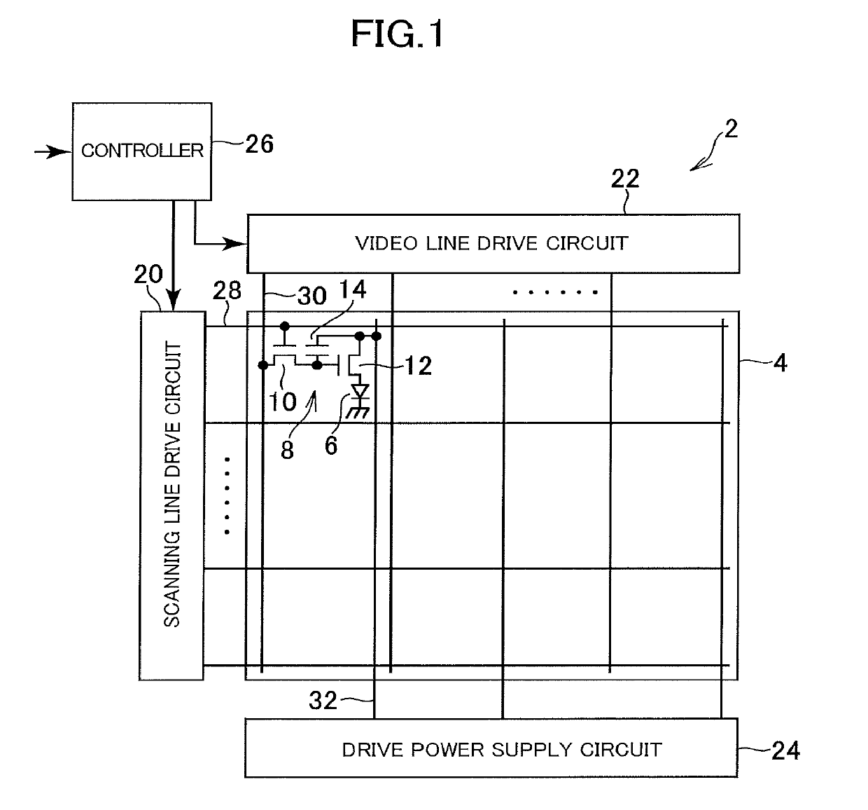
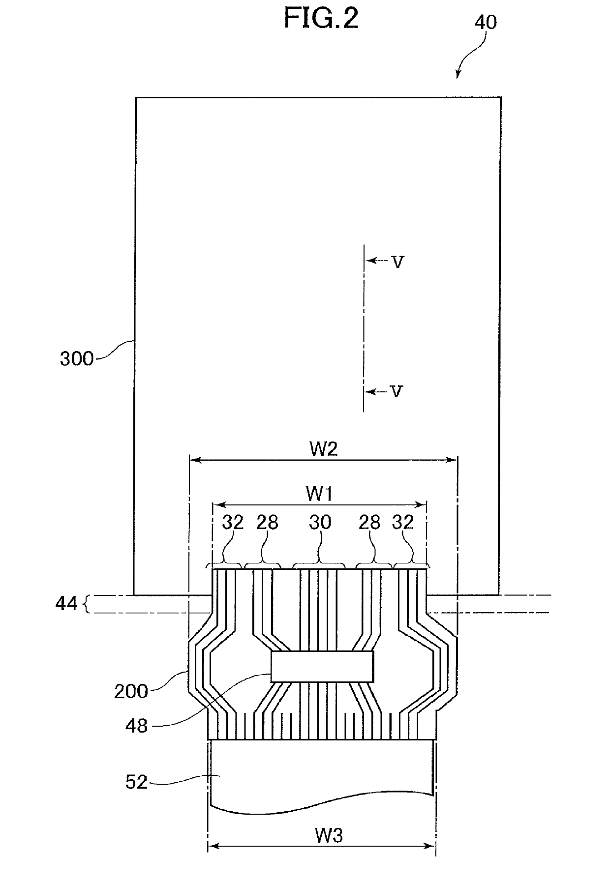
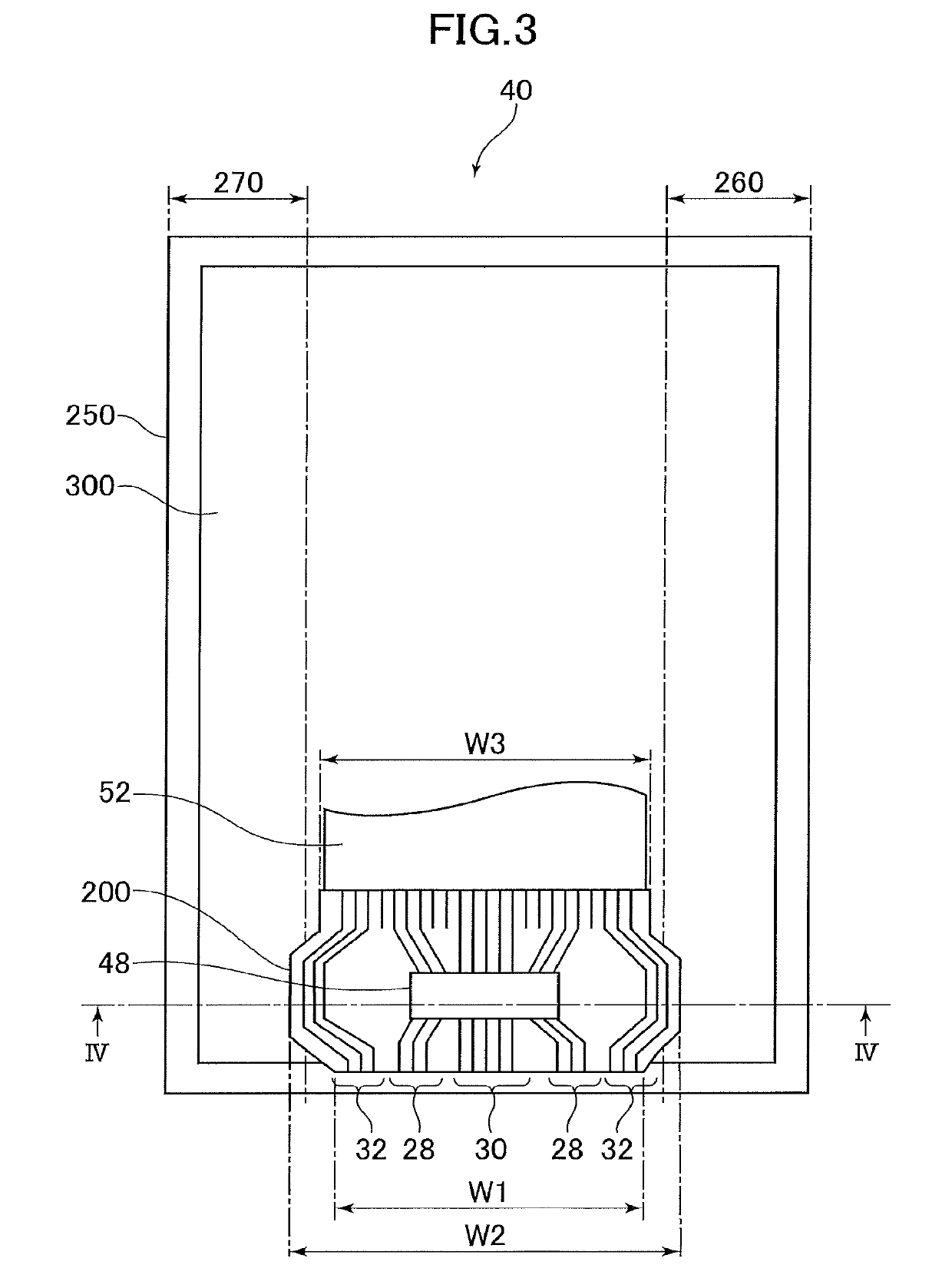
[0025]A display device 2 according to the embodiment is, for example, an org...


PUM


Abstract

There is provided a display device including an organic light-emitting diode structure layer including a pixel array section, a film connected to a first edge-side region of the organic light-emitting diode structure layer and folded back onto a rear surface side of the organic light-emitting diode structure layer, and an integrated circuit disposed on the film. A width of the film in a connection region to the organic light-emitting diode structure layer is smaller than a width of the film in a region where the integrated circuit is disposed.

Description

CROSS-REFERENCE TO RELATED APPLICATION[0001]The present application claims priority from the Japanese Application JP2017-117412 filed on Jun. 15, 2017, the content of which is hereby incorporated by reference into this application.BACKGROUND OF THE INVENTION1. Field of the Invention[0002]The present invention relates to a display device.2. Description of the Related Art[0003]A flat panel display such as an organic electroluminescence (EL) display device includes a display panel in which thin film transistors (TFTs), organic light-emitting diodes (OLEDs), and the like are formed on a substrate. A glass substrate has been conventionally used for a base material of the display panel. In recent years, however, a flexible display in which the display panel can be bent is being developed with use of a resin film or the like such as a polyimide film for the base material.[0004]As applications of the flexible display, it is considered to achieve a narrower picture frame by folding a chip on...

Claims


Application Information

Patent Timeline
Patent Type & Authority Patents(United States)
IPC IPC(8): H01L51/00H01L51/52H01L27/32
CPCH01L51/5237H01L51/0097H01L27/3276H01L2251/5338Y02E10/549H10K59/131H10K77/111H10K2102/311H10K59/87H10K50/84
Inventor FUJIOKA, TAKAHIROKATO, KENGO
Owner JAPAN DISPLAY INC
Why Eureka
Try Eureka