
High gain load circuit for a differential pair using depletion mode transistors

a depletion-mode transistor and high-gain load technology, applied in the field of depletion-mode transistors, can solve the problems of limited gan transistor device choice, inability to manufacture p-type gan devices, and limited technology, so as to achieve enhanced differential pair gain stage and increase output impedance

Active Publication Date: 2019-05-07
ANALOG DEVICES INC
View PDF15 Cites 1 Cited by
  • Summary
  • Abstract
  • Description
  • Claims
  • Application Information

AI Technical Summary

Benefits of technology

The invention describes a technical solution to improve the performance of analog circuitry by using a differential pair of transistors. This configuration helps to enhance the gain of the transistors and increase the output impedance. By using a cascode stage, the transistors in the active load have a constant voltage, which in turn results in an increased output impedance. This results in a more efficient and effective analog circuit design.

Problems solved by technology

Some fabrication technologies are either technically limited or cost limited to fabricating only depletion mode field effect transistors.
The variety of GaN transistor device choices, however, is limited.
While n-type depletion and enhancement mode devices are available, p-type GaN devices are not available as they have poor performance due to fundamental device physics issues.
Hence the challenge is to make analog circuits using only n-type depletion and enhancement mode devices.
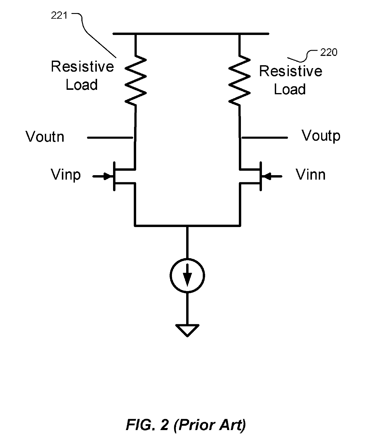
This circuit has poor gain because the resistors 220, 221 cannot be made sufficiently large as the resistor has to conduct the DC bias current, thus the resistors need to be small.
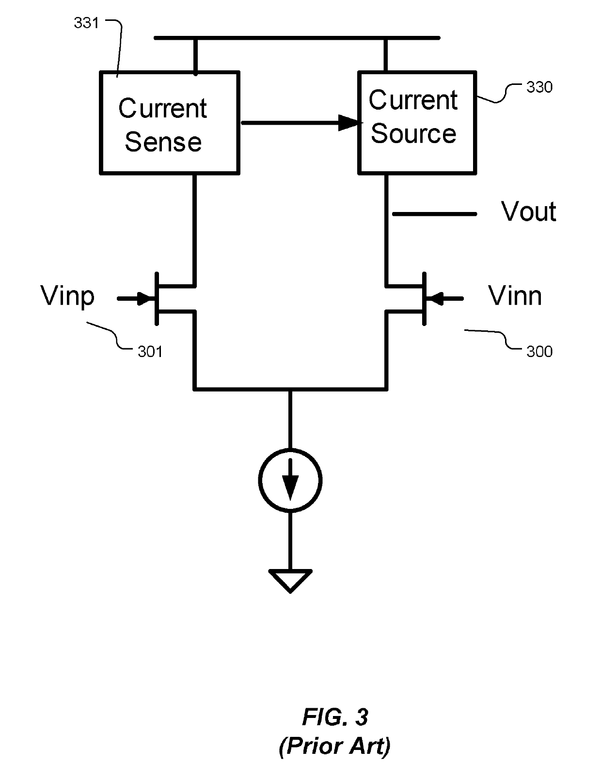
Undesirably, this option currently is not available in the GaN fabrication process.

Method used


Image

  • High gain load circuit for a differential pair using depletion mode transistors
  • High gain load circuit for a differential pair using depletion mode transistors
  • High gain load circuit for a differential pair using depletion mode transistors

Examples


Embodiment Construction

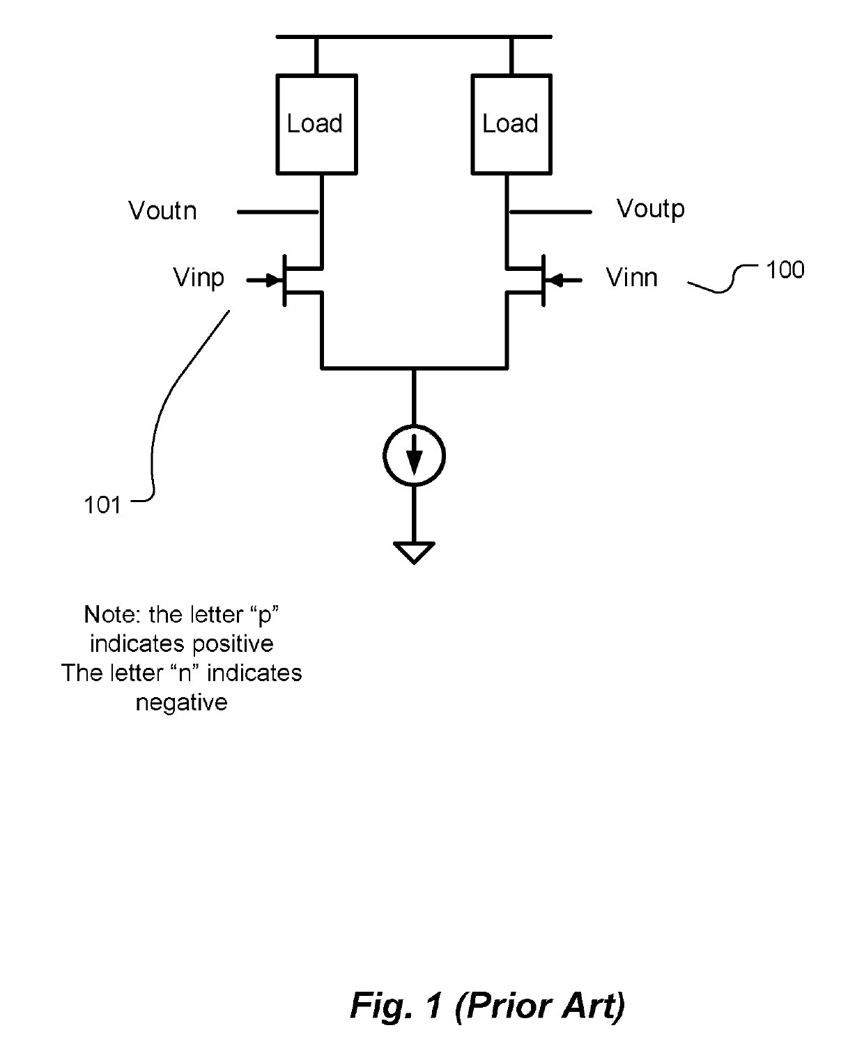
[0010]Embodiments of the invention include a depletion mode differential pair gain stage. The gain stage includes a differential pair of depletion-mode transistors, including a first and a second n-type transistor. In certain embodiments of the invention, the depletion mode transistor may be GaN (gallium nitride) field effect transistors. The transistors have a gate, source, and a drain and the differential pair coupled at the source of each transistor forming a common node. The gain stage also includes an active load including one or more depletion mode transistors electrically coupled to at least one of the drains of depletion mode transistors of the differential pair.

[0011]The differential pair may also include a constant current source coupled to a common node of the differential pair. The current source can be used for biasing the differential pair.

[0012]In embodiments of the invention, the active load includes a current source formed from a third depletion mode transistor coup...


PUM


Abstract

A differential pair gain stage is disclosed. In one embodiment, the gain stage includes a differential pair of depletion-mode transistors, including a first and a second n-type transistor. In certain embodiments of the invention, the depletion mode transistor may be GaN (gallium nitride) field effect transistors. The gain stage includes an active load including one or more depletion mode transistors electrically coupled to at least one of the drains of depletion mode transistors of the differential pair. The active load may include a source follower for maintaining the AC voltages at the drains of the differential pair at a constant value and may further include a casocde stage for setting a fixed drain source voltage across the output transistors to increase the output impedance and gain of the stage.

Description

PRIORITY[0001]The present application claims the benefit of U.S. Provisional Patent Application 62 / 087,987 filed on Dec. 5, 2014, which is incorporated herein by reference in its entirety.FIELD OF THE INVENTION[0002]The invention generally relates to depletion mode transistors and, more particularly, the invention relates to a differential pair gain stage using depletion mode transistors, such as, gallium nitride transistors.BACKGROUND OF THE INVENTION[0003]As should be understood by one of ordinary skill in the art, depletion mode field effect transistors are in an “on” state when the gate voltage is equal to the source voltage of the transistor, such that current will flow through the drain source juncture of the transistor. A depletion mode device can be turned “off” when the gate voltage is taken below the source voltage by the threshold voltage when current stops flowing through the drain source junction of the transistor.[0004]Some fabrication technologies are either technical...

Claims


Application Information

Patent Timeline
Patent Type & Authority Patents(United States)
IPC IPC(8): H03K5/22H01L29/20H03F3/45H01L27/088H03K17/687
CPCH03K17/6871H01L29/2003H03F3/45188H03F3/45385H01L27/088H03F2203/45722H03F2200/303H03F2200/75H03F2203/45036H03F2203/45182H03F2203/45184H03F2203/45188H03F2203/45202H03F2203/45208H03F2203/45224H03F2203/45656H03F2203/45674H03F2203/45676H03F2203/45701H03F2203/45702
Inventor SHARMA, YOGESH JAYARAMANFIORENZA, JAMES
Owner ANALOG DEVICES INC
Learn More