Semiconductor device and electronic device
a semiconductor device and electronic device technology, applied in the direction of pulse technique, power consumption reduction, testing/measurement of semiconductor/solid-state devices, etc., can solve the problems of reducing the output voltage by a threshold voltage, increasing manufacturing costs, and reducing the productivity of semiconductor devices, so as to achieve high productivity and low power consumption , the effect of reliable semiconductor devices
- Summary
- Abstract
- Description
- Claims
- Application Information
AI Technical Summary
Benefits of technology
Problems solved by technology
Method used
Image

Examples
embodiment 1
(Embodiment 1)
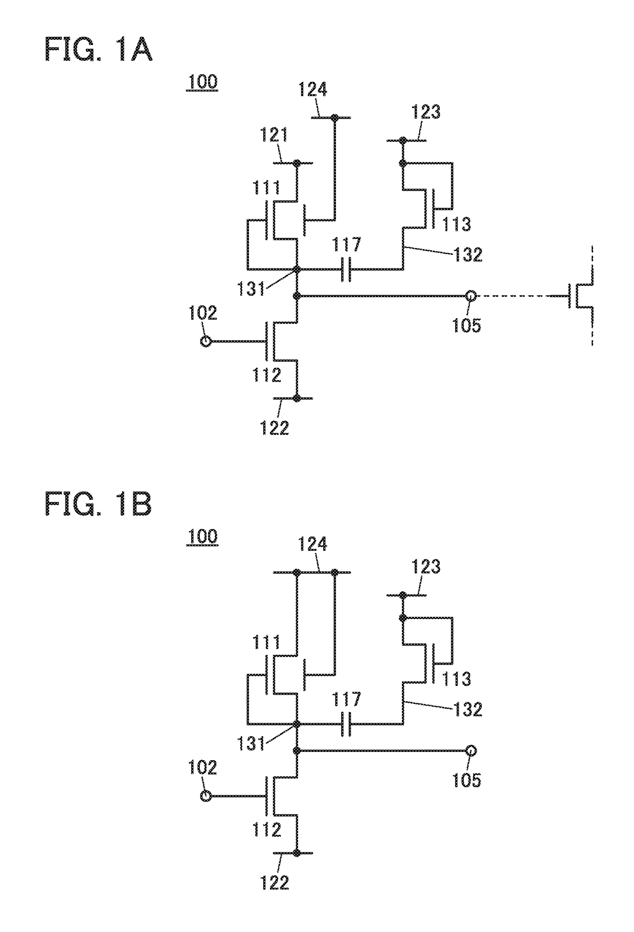
[0085]In this embodiment, a semiconductor device 100 of one embodiment of the present invention will be described with reference to drawings. FIG. 1A is a circuit diagram illustrating a structure of the semiconductor device 100.
100>
[0086]The semiconductor device 100 includes transistors 111 to 113 and a capacitor 117. The transistors 111 to 113 are each an n-channel transistor including a source, a drain, and a gate. The transistor 111 includes a back gate in addition to the gate. The transistor 112 and / or the transistor 113 can be provided with a back gate.
[0087]The gate and the back gate are located so that a channel formation region in a semiconductor layer is sandwiched therebetween. Thus, the back gate can function in a manner similar to that of the gate. The potential of the back gate may be the same as that of the gate or may be a ground (GND) potential or a predetermined potential. By changing the potential of the back gate independently of the potential of the...
embodiment 2
(Embodiment 2)
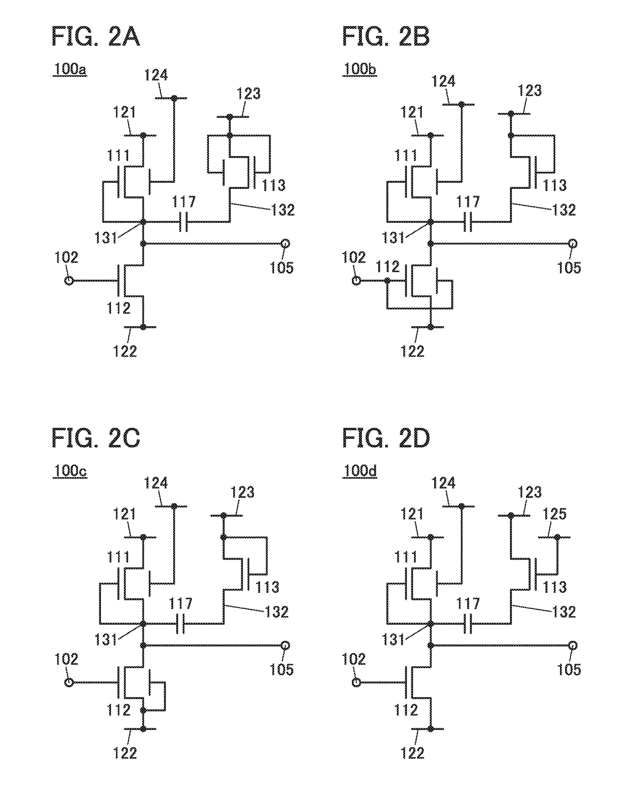
[0105]In this embodiment, a semiconductor device 110 having a different structure from that of the semiconductor device 100 will be described with reference to drawings. FIG. 7A is a circuit diagram showing the structure of the semiconductor device 110. In this embodiment, a description is mainly made of portions different from the semiconductor device 100 to avoid repetition of the same description. For parts that are not described in this embodiment, the other embodiments or common general technical knowledge known to those skilled in art can be referred to.
110>
[0106]The semiconductor device 110 has a structure in which a back gate is additionally provided for the transistor 113 that is the same as in the semiconductor device 100 in FIG. 1A, and the back gate is electrically connected to the other of the source and the drain of the transistor 113.
[0107]Note that an inverted signal of a signal inputted to the terminal 102 may be inputted to the wiring 121. In this cas...
embodiment 3
(Embodiment 3)
[0122]In this embodiment, a semiconductor device 120 having a structure different from that of the semiconductor device 100 will be described with reference to drawings. FIG. 12A is a circuit diagram showing the structure of the semiconductor device 120. In this embodiment, a description is made of portions different from the semiconductor device 100 to avoid repetition of the same description. For parts that are not described in this embodiment, the other embodiments or common general technical knowledge known to those skilled in art can be referred to.
120>
[0123]The semiconductor device 120 has a structure in which a transistor 114 is added to the semiconductor device 100 shown in FIG. 1A. In the transistor 114 in the semiconductor device 120, one of a source and a drain is electrically connected to the node 132, and the other of the source and the drain is electrically connected to the wiring 122. A gate of the transistor 114 is electrically connected to the terminal...
PUM
 Abstract
Description
Claims
Application Information
 - R&D
- Intellectual Property
- Life Sciences
- Materials
- Tech Scout
- Unparalleled Data Quality
- Higher Quality Content
- 60% Fewer Hallucinations
Browse by: Latest US Patents, China's latest patents, Technical Efficacy Thesaurus, Application Domain, Technology Topic, Popular Technical Reports.
© 2025 PatSnap. All rights reserved.Legal|Privacy policy|Modern Slavery Act Transparency Statement|Sitemap|About US| Contact US: help@patsnap.com