
Semiconductor rectifier and manufacturing method thereof

a technology of semiconductors and rectifiers, applied in the direction of dc-dc conversion, power conversion systems, instruments, etc., can solve the problems of increasing circuit loss, allowing currents to pass through, and their manufacturing process is not compatible with silicon, so as to achieve significant forward voltage drop of devices, reverse voltage increase, and reverse leakage of devices low

Active Publication Date: 2018-08-28
CSMC TECH FAB2 CO LTD
View PDF10 Cites 0 Cited by
  • Summary
  • Abstract
  • Description
  • Claims
  • Application Information

AI Technical Summary

Benefits of technology

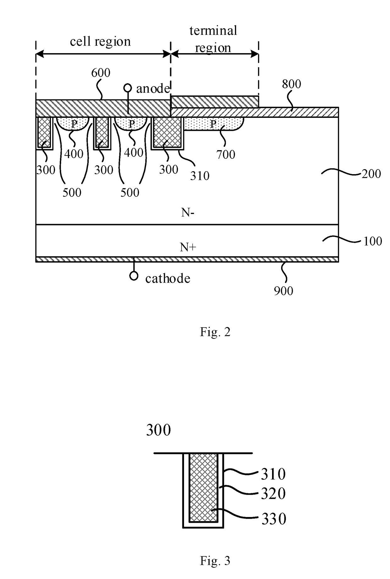
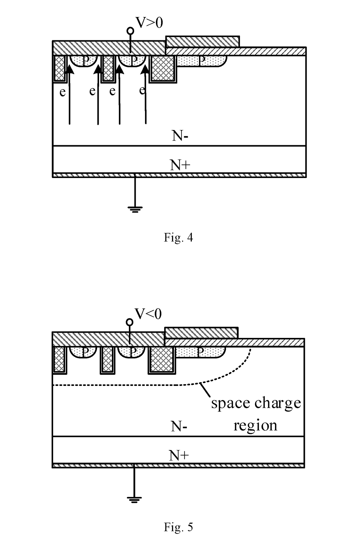
The patent describes a semiconductor rectifying device with low forward voltage drop, low reverse leakage, high reverse breakdown voltage, and high avalanche ruggedness. The device has a filling structure that allows for electron enhancement, reducing the potential barrier to electronic movement and lowering the forward voltage drop. When the device is reverse biased, a space charge region formed by a p-n junction and a filling structure blocks carrier movement, reducing reverse leakage and increasing the reverse breakdown voltage and avalanche ruggedness. The manufacturing process is compatible with a trench MOS process and requires four photomasks, simplifying the process and reducing manufacturing costs.

Problems solved by technology

Semiconductor diodes have such characteristics that when voltage is forward biased, they allow electric currents to pass through, and when the voltage is reverse biased, they do not allow the currents to pass through.
The forward voltage drop of germanium p-n junction diodes is about 0.3 V, but their manufacturing process is not compatible with silicon process, and they are very sensitive to temperature, so they are not widely applied.
The leakage will increase circuit loss, reduce circuit conversion efficiency, especially in high temperature applications.
Reverse voltage generated by the inductors may be applied to a diode, leading to an avalanche breakdown of the diode.
The presence of each filling structure increases the size of a junction area for energy dissipation of the device, thus allowing the device to have high reverse breakdown voltage and high avalanche ruggedness.

Method used


Image

  • Semiconductor rectifier and manufacturing method thereof
  • Semiconductor rectifier and manufacturing method thereof
  • Semiconductor rectifier and manufacturing method thereof

Examples


Embodiment Construction

[0025]Embodiments of the disclosure are described more fully hereinafter with reference to the accompanying drawings. The various embodiments of the disclosure may, however, be embodied in many different forms and should not be construed as limited to the embodiments set forth herein. Rather, these embodiments are provided so that this disclosure will be thorough and complete, and will fully convey the scope of the disclosure to those skilled in the art.

[0026]Unless otherwise defined, all terms (including technical and scientific terms) used herein have the same meaning as commonly understood by one of ordinary skill in the art to which this disclosure belongs. It will be further understood that terms, such as those defined in commonly used dictionaries, should be interpreted as having a meaning that is consistent with their meaning in the context of the relevant art and will not be interpreted in an idealized or overly formal sense unless expressly so defined herein. As used herein...


PUM

PropertyMeasurementUnit
energyaaaaaaaaaa
thicknessaaaaaaaaaa
forward voltage dropaaaaaaaaaa

Abstract

A semiconductor rectifying device includes a substrate of a first conductivity type, an epitaxial layer of the first conductivity type, a filling structure, an upper electrode, a guard ring, and a guard layer. The epitaxial layer defines a plurality of trenches thereon. The filling structure includes an insulating material formed on the inner surface of the trench and a conductive material filled in the trench. A doped region of a second conductivity type is formed in the surface of the epitaxial layer between the filling structures. A method of manufacturing a semiconductor rectifying device includes forming an epitaxial layer of a first conductivity type on a substrate of the first conductivity type, defining a plurality of trenches on the epitaxial layer, forming a plurality of filling structures in the plurality of trenches, and forming a doped region in the epitaxial layer between the filling structures.

Description

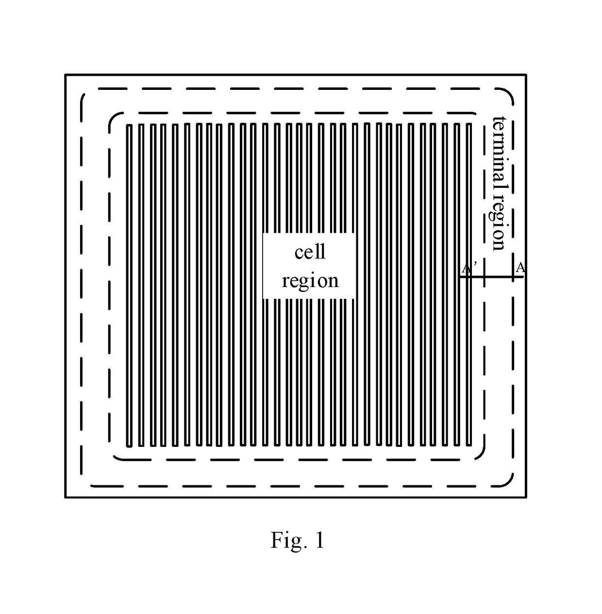
FIELD OF THE INVENTION[0001]The present disclosure relates to the field of semiconductor device, and particularly relates to a semiconductor rectifying device and a manufacturing method thereof.BACKGROUND OF THE INVENTION[0002]Semiconductor diodes have such characteristics that when voltage is forward biased, they allow electric currents to pass through, and when the voltage is reverse biased, they do not allow the currents to pass through. Semiconductor diodes are widely used in various types of electronic circuits such as power supply circuits, signal processing circuits and so on. For a particular type of diode, a forward current is substantially negligible until a forward voltage drop reaches a certain value. For example, silicon p-n junction diodes have a forward voltage drop of at least around 0.7 V. The forward voltage drop of many silicon Schottky barrier diodes can be 0.4 V or even lower owing to Schottky barrier characteristics. The forward voltage drop of germanium p-n ju...

Claims


Application Information

Patent Timeline
Patent Type & Authority Patents(United States)
IPC IPC(8): H01L29/06H02M3/158H01L29/861H01L21/04H01L21/02H01L21/78H01L21/768
CPCH01L29/06H01L21/02293H01L21/041H01L21/78H01L29/861H02M3/1588H01L21/76877H01L21/02378H01L29/407H01L29/6609H01L29/0619
Inventor ZHONG, SHENGRONGDENG, XIAOSHEZHOU, DONGFEI
Owner CSMC TECH FAB2 CO LTD
Learn More