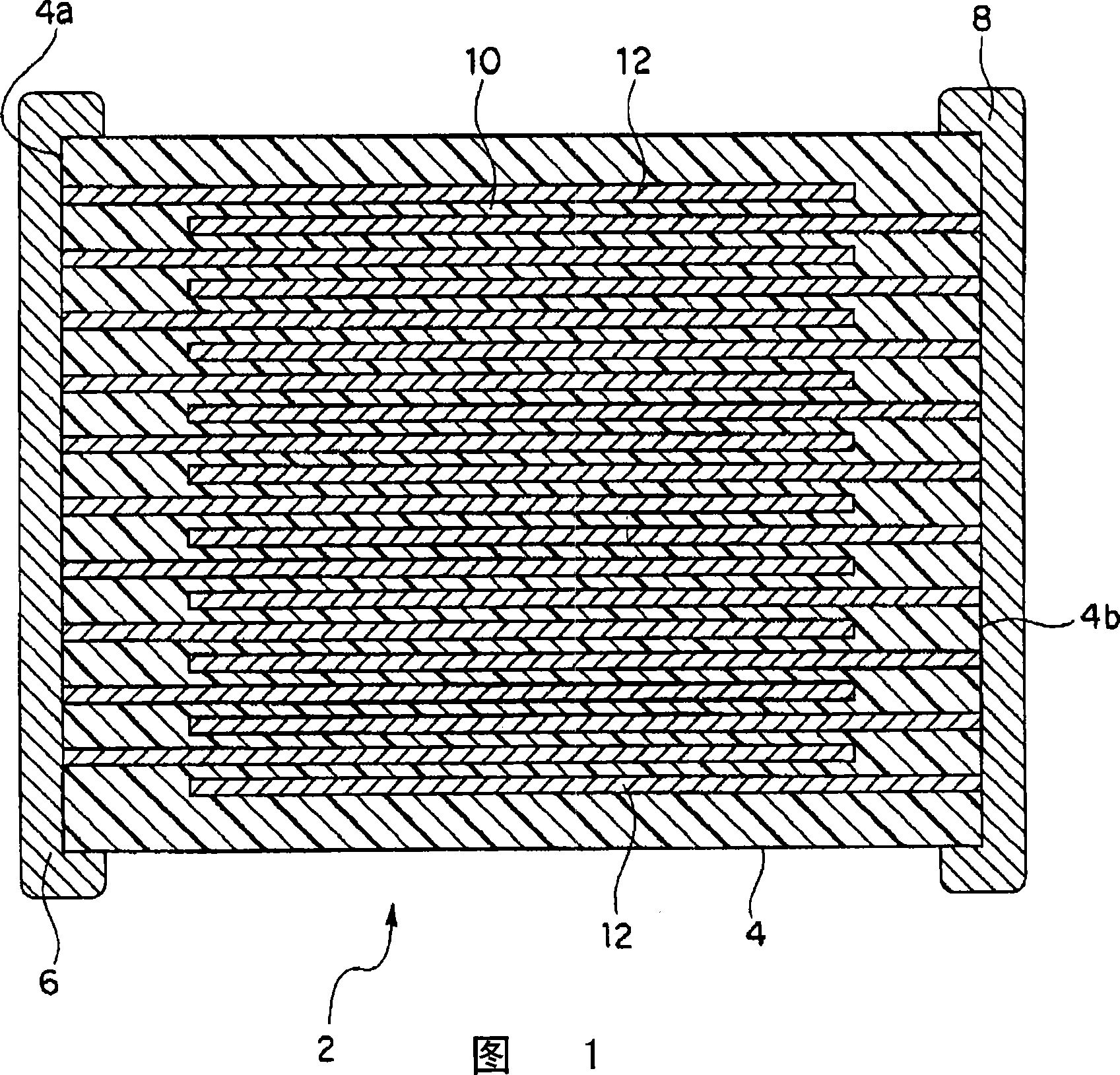
Electronic part, layered ceramic capacitor, and manufacturing method thereof
A technology of ceramic capacitors and electronic components, which is applied in the direction of laminated capacitors, capacitors, fixed capacitors, etc., can solve the problem of reduced electrostatic capacity, and achieve the effect of preventing electrode discontinuity and suppressing the reduction of electrostatic capacity
- Summary
- Abstract
- Description
- Claims
- Application Information
AI Technical Summary
Problems solved by technology
Method used
Image
Examples
Embodiment 1
[0143] Preparation of each paste
[0144] First, the BaTiO 3 Powder (BT-02 / Sakai Chemical Industry Co., Ltd.) and MgCO 3 , MnCO 3 , (Ba 0.6 Ca 0.4 ) SiO 3 And selected from rare earths (Gd 2 o 3 , Tb 4 o 7 、Dy 2 o 3 、Ho 2 o 3 、Er 2 o 3 、Tm 2 o 3 , Yb 2 o 3 、Lu 2 o 3 , Y 2 o 3 ) powder was wet-mixed by ball milling for 16 hours, and then dried to make a dielectric material. The average particle diameter of these raw material powders is 0.1-1 μm. (Ba 0.6 Ca 0.4 ) SiO 3 is the BaCO 3 , CaCO 3 and SiO 2It was wet-mixed by ball milling for 16 hours, dried and sintered in air at 1150° C., and then wet pulverized by ball milling for 100 hours.
[0145] In order to form the obtained dielectric material into a paste, the organic vehicle was added to the dielectric material and mixed by a ball mill to obtain a paste for dielectric green sheets. The organic vehicle is polyvinyl butyral as a binder: 6 parts by mass, bis(2-ethylhexyl) phthalate (DOP) as a pla...
Embodiment 2
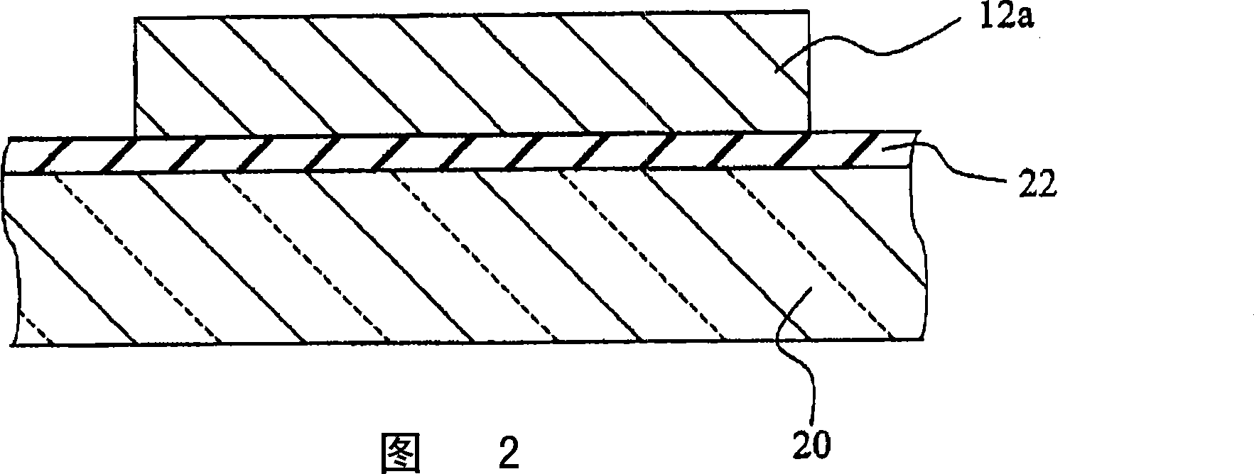
[0196] The dielectric green sheet paste prepared in Example 1 was coated on a PET film (carrier sheet) using a wire bar coater, and then dried to obtain a green sheet 10a. The same procedure as in Example 1 was carried out. In this method, a pre-sintered internal electrode thin film 12a is formed on the green sheet 10a to prepare a laminate as shown in FIG. 8 . Next, the PET film was peeled off from the laminate to prepare a pre-sintered sample composed of the green sheet 10a and the internal electrode film 12a, and the pre-sintered sample was debindered and sintered in the same manner as in Example 1. and annealing to prepare a sintered surface observation sample composed of the dielectric layer 10 and the internal electrode layer 12 .
[0197]Next, the obtained sample for surface observation was observed by SEM from a direction perpendicular to the surface on which the internal electrode layer 12 was formed, and the internal electrode layer after sintering was observed and e...
Embodiment 3
[0201] In the formation of the internal electrode film 12a before firing, Yb 2 o 3 Instead of BaTiO used as a dielectric target 3 , except that, a sample was obtained in the same manner as in Example 1. The characteristics evaluation of the electrical characteristics (capacitance C, dielectric loss tan δ) was performed for each sample. The results are shown in Table 2. Electrical characteristics (capacitance C, dielectric loss tan δ) were performed in the same manner as in Example 1.
[0202]
sample
serial number
Internal electrode film 12a before sintering
Capacitance
[µF]
tanδ
Evaluation
thickness
[μm]
Nickel content ratio
[wt%]
Yb 2 o 3 contains
Proportion [wt%]
6
comparative example
0.4
100
0.0
0.83
0.01
×
7
Example
0.4
99.30
0.70
0.97
0.02
○
8
...
PUM
| Property | Measurement | Unit |
|---|---|---|
| thickness | aaaaa | aaaaa |
| particle size | aaaaa | aaaaa |
| particle size | aaaaa | aaaaa |
Abstract
Description
Claims
Application Information
 - R&D
- Intellectual Property
- Life Sciences
- Materials
- Tech Scout
- Unparalleled Data Quality
- Higher Quality Content
- 60% Fewer Hallucinations
Browse by: Latest US Patents, China's latest patents, Technical Efficacy Thesaurus, Application Domain, Technology Topic, Popular Technical Reports.
© 2025 PatSnap. All rights reserved.Legal|Privacy policy|Modern Slavery Act Transparency Statement|Sitemap|About US| Contact US: help@patsnap.com


