Stage assembly, particle-optical apparatus comprising such a stage assembly, and method of treating sample
A workbench and component technology, applied in scientific instruments, electrical components, semiconductor/solid-state device manufacturing, etc., can solve problems such as uneven processing results
- Summary
- Abstract
- Description
- Claims
- Application Information
AI Technical Summary
Problems solved by technology
Method used
Image


Examples
Embodiment 1
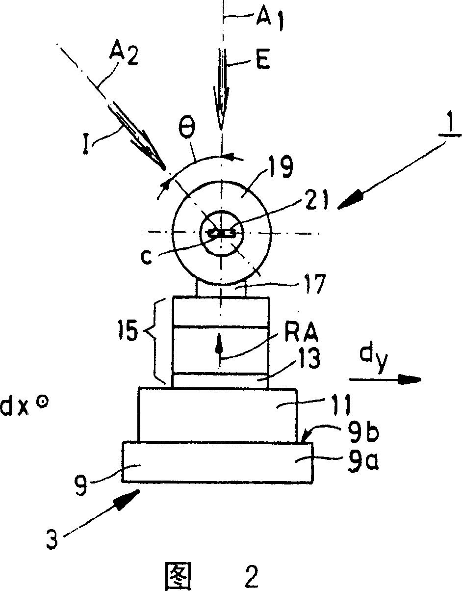
[0045] Figure 1 shows a partial front view of one embodiment of a particle optics device 1 and stage assembly 3 of the present invention. Workbench assembly 3 among the figure is made up of following elements:
[0046] - a sub-table 5 that can move back and forth along the direction dx parallel to the X-axis;
[0047] - the main rotating part 7 mounted on the sub-table 5 for rotating the frame 9 around the main axis PA parallel to the X-axis;
[0048] - a part 11 supported by the frame 9 for moving the slide 13 back and forth in translation relative to the frame 9 in a direction dy parallel to the Y-axis;
[0049] - a Z-member 15 supported by a slide 13 for rotating the platform 17 about the axis of rotation RA and for translation of the platform 17 along this axis of rotation RA. With reference to the frame 9, the axis of rotation RA is parallel to the Z-axis.
[0050] - A turning member 19 supported by the platform 17 for rotating the sample stage 21 about the turning axi...
Embodiment 2
[0059] Another embodiment of the particle optics device and workbench assembly of the present invention is the same as Embodiment 1 above, except that the frame 9 cannot rotate around the main axis. In such a non-concentric arrangement, the axis of rotation RA is permanently parallel to, for example, the first axis A 1 .
Embodiment 3
[0061] Another embodiment of the particle optical device and workbench assembly of the present invention is the same as the above-mentioned embodiment 1, except that the workbench assembly 3 is equipped with an additional mechanism 3' on the slide plate 13. The sample stage 21 among Fig. 1 and 2 is used to support very small microscopic size (for example 30 * 30 * 0.1 μ m 3 ) sample, and the sample holder 21B in the additional mechanism 3' is used to support bulky samples, such as the major part of a whole semiconductor wafer (such as diameter 100mm and thickness 1.2mm). To this end, the mechanism 3' comprises a large-dimension Z-part 15B supported by the slide 3 for rotating the sample carrier 21B around the mass axis of rotation 25 and for aligning the sample carrier 21B along the mass axis of rotation 25. move. This mass axis of rotation 25 is parallel to the axis of rotation RA and is a fixed distance away from it. In this case, the stroke of the Y component is sufficien...
PUM
| Property | Measurement | Unit |
|---|---|---|
| thickness | aaaaa | aaaaa |
Abstract
Description
Claims
Application Information
 - R&D
- Intellectual Property
- Life Sciences
- Materials
- Tech Scout
- Unparalleled Data Quality
- Higher Quality Content
- 60% Fewer Hallucinations
Browse by: Latest US Patents, China's latest patents, Technical Efficacy Thesaurus, Application Domain, Technology Topic, Popular Technical Reports.
© 2025 PatSnap. All rights reserved.Legal|Privacy policy|Modern Slavery Act Transparency Statement|Sitemap|About US| Contact US: help@patsnap.com