New structure crystal silicon solar energy battery
A technology of solar cells and crystalline silicon, which is applied in the field of solar energy applications, and can solve the problems of carrier depletion in the emission area, reduction of cell efficiency, and drop in cell efficiency
- Summary
- Abstract
- Description
- Claims
- Application Information
AI Technical Summary
Problems solved by technology
Method used
Image

Examples
Embodiment Construction
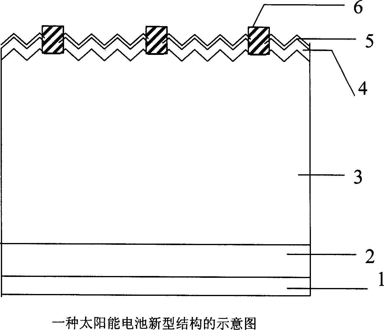
[0012] Technical solution: high-quality N-type monocrystalline silicon wafer (3) is used, the thickness is less than 300 μm, and the resistivity is 5-500 Ωcm. After the surface is cleaned and textured by standard industrial processes, a layer of highly doped N + Layer (4), with a sheet resistance of 100-300Ω / □ (the function of this layer is to passivate the front surface of the battery by utilizing the change of doping concentration, and provide good ohmic contact for the front surface electrode at the same time). in N + Deposit or grow a thin film (5) with anti-reflection effect on the layer, such as SiN or SiO 2 etc., the thickness is 70-120nm. A silicon thin film (2), such as amorphous silicon, microcrystalline silicon, or nanocrystalline silicon, is deposited on the back of the N-type single crystal silicon wafer (3), with a thickness of 20-200nm. Finally, a positive electrode (6) is prepared on the antireflection layer (5), and a negative electrode (1) is prepared on t...
PUM
 Abstract
Description
Claims
Application Information
 - R&D
- Intellectual Property
- Life Sciences
- Materials
- Tech Scout
- Unparalleled Data Quality
- Higher Quality Content
- 60% Fewer Hallucinations
Browse by: Latest US Patents, China's latest patents, Technical Efficacy Thesaurus, Application Domain, Technology Topic, Popular Technical Reports.
© 2025 PatSnap. All rights reserved.Legal|Privacy policy|Modern Slavery Act Transparency Statement|Sitemap|About US| Contact US: help@patsnap.com