
Semiconductor memory

A semiconductor and memory technology, applied in the field of semiconductor memory, can solve problems such as failure to meet specifications and increase power consumption

Inactive Publication Date: 2007-04-04
SHARP KK +1
View PDF1 Cites 8 Cited by
  • Summary
  • Abstract
  • Description
  • Claims
  • Application Information

AI Technical Summary

Problems solved by technology

[0013] However, in the current flash memory standard, it is necessary to output DQ at several clocks from the synchronous read, and there is a problem that the conventional DLL circuit such as the above-mentioned DLL circuit cannot meet this standard.
Alternatively, in order to meet the current flash memory specifications, it is conceivable to input an external clock even during backup and perform phase correction in the DLL circuit at all times, but this will cause a problem that the power consumption will increase unnecessarily.

Method used


Image

  • Semiconductor memory
  • Semiconductor memory
  • Semiconductor memory

Examples


Embodiment Construction

[0056] Hereinafter, preferred modes for implementing the present invention will be described with reference to the drawings.

[0057] "Semiconductor Memory Circuits"

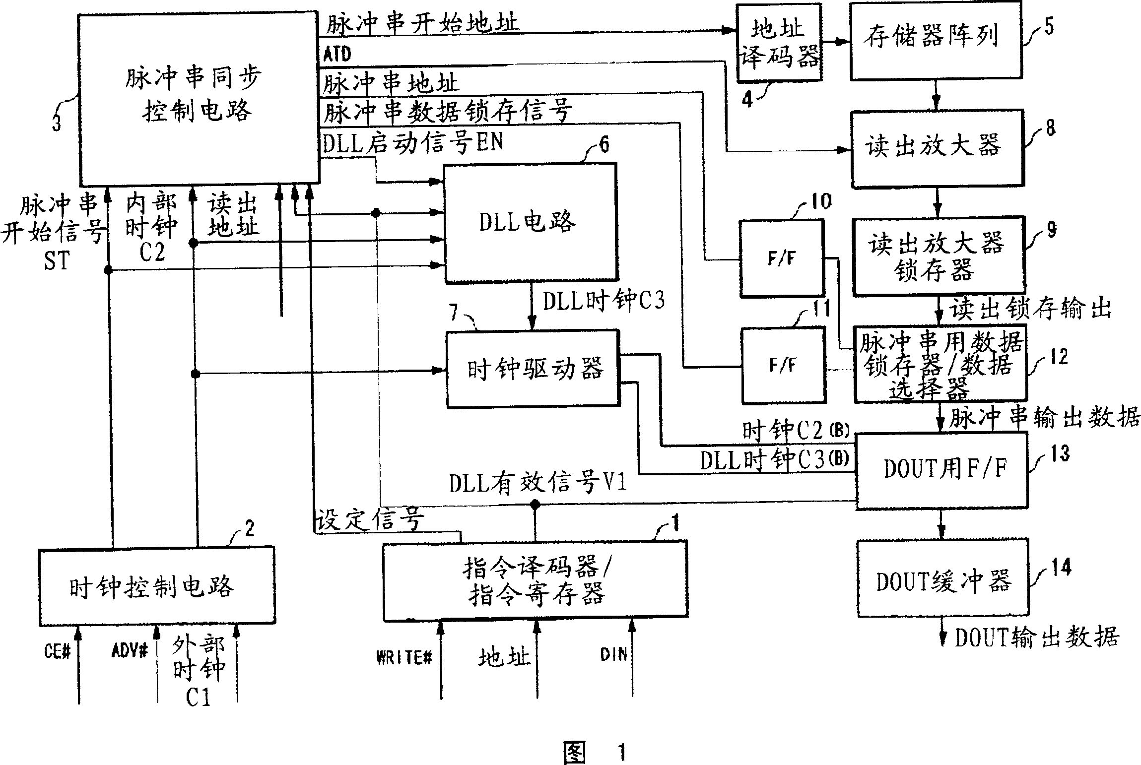
[0058] FIG. 1 is a diagram showing a configuration example (synchronous readout system) of a semiconductor memory in an embodiment of the present invention, and shows an example of a flash memory. In addition, "#" at the end of each signal indicates that it is valid at negative logic "L".

[0059] In Fig. 1, the instruction decoder / instruction register 1 decodes the address and DIN and determines the instruction, and uses the instruction write signal WRITE# to store the judgment result in the register. Also, set the type of burst mode, clock latency, and use / non-use of DLL. A DLL valid signal (a signal indicating use / non-use of DLL) V1 input based on a user command is output to the burst synchronization control circuit 3 , the DLL circuit 6 , and the flip-flop for DOUT (F / F for DOUT) 13 . In addition, a setti...


PUM


Abstract

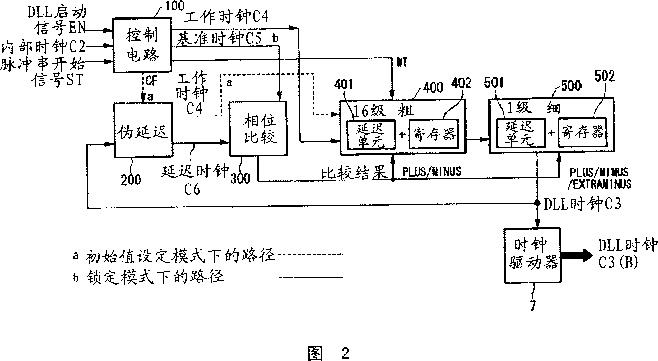
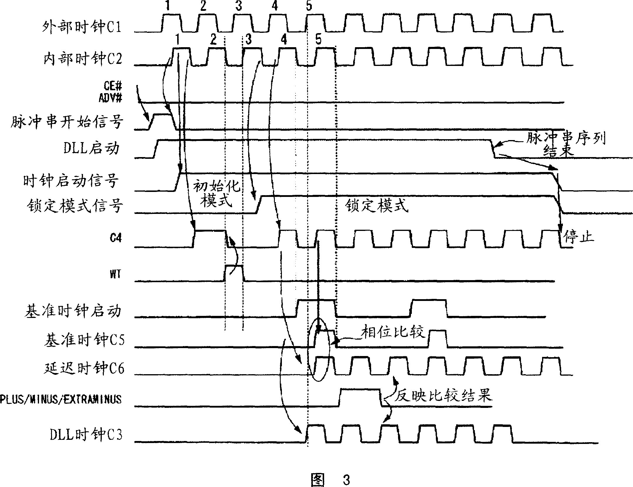
A semiconductor memory using a DLL circuit having a phase comparison circuit for comparing phases of an internal clock and a delay clock and a variable delay addition circuit for adjusting delay amount according to a signal from the phase comparison circuit comprises a means for inputting a first signal latched to a logic "1" by start of one clock cycle of the internal clock to the variable delay addition circuit through a dummy delay at the start of burst and a means for detecting the duration time of the logic "1" of the first signal inputted by the variable delay addition circuit through the dummy delay until one clock cycle of the internal clock is completed and setting the initial value of delay amount of the variable delay addition circuit based on the duration time.

Description

technical field [0001] The present invention relates to a semiconductor memory, especially a flash memory, which ensures synchronization of an external clock and a DQ output (memory data output) even at a high-speed clock. Background technique [0002] In recent years, the demand for flash memory has rapidly expanded as a nonvolatile memory. Under such circumstances, the speed-up of the reading speed is progressing, and it is urgently required to operate at a clock frequency exceeding 100 MHz for practical use. Therefore, even in a flash memory, a structure for canceling an internal clock delay becomes indispensable. So far, although there is no structure targeting flash memory, various DLL (Delay Locked Loop: Delay Locked Loop) circuits are provided or proposed (for example, refer to Patent Document 1). [0003] Patent Document 1: JP-A-2001-326563 [0004] Next, the necessity of the DLL circuit will be described with reference to FIG. 17 . FIG. 17 ...

Claims


Application Information

Patent Timeline
Patent Type & Authority Applications(China)
IPC IPC(8): G11C16/32G11C11/4063G01F1/12H03H11/26H03L7/08G11C16/02G06F1/12G11C7/10G11C11/407G11C11/4076G11C16/06G11C29/02H03K5/00H03K5/14H03K5/26H03L7/081
CPCG11C29/50012G11C7/1072H03L7/0818G11C16/32G11C7/222H03K2005/00019H03K5/132H03L7/0814H03K5/133G11C2207/2254G11C29/02G11C29/028G11C16/06
Inventor 前田贤吾谷川明西山增治大堀庄一平野诚高岛洋的场伸次浅野正通
Owner SHARP KK
Learn More