Heat elimination type structure for packing complex crystal

A technology of flip-chip packaging and heat dissipation, which is applied in the direction of electrical components, electric solid-state devices, circuits, etc., and can solve problems such as product failure, product impact on performance, and inconvenience

Inactive Publication Date: 2007-02-21
CHIPMOS TECH INC
View PDF0 Cites 6 Cited by
  • Summary
  • Abstract
  • Description
  • Claims
  • Application Information

AI Technical Summary

Problems solved by technology

The solder balls 20 are disposed on the lower surface 11 of the substrate 10, the flip chip 30 is disposed on the upper surface 12 of the substrate 10, and the bumps 40 are formed on an active surface 31 of the flip chip 30 to electrically connect the substrate. 10 and the flip chip 30, the heat sink 50 is arranged on the upper surface 12 of the substrate 10 through a stiffener 60, and is thermally coupled with a back surface 32 of the flip chip 30, wherein the thermal energy generated by the flip chip 30 is conducted to the heat sink 50, and then dissipate heat energy through the heat sink 50, so the size of the heat sink 50 is the most important key for the entire component, and the above-mentioned flip-chip chip 30 only dissipates heat energy through the heat sink 50, when the When the heat sink 50 is installed on a heat source with a high temperature, the heat energy of the heat source cannot be dissipated in time due to the insufficient heat dissipation area of ​​the heat sink 50, which will cause the product temperature to be too high and affect the performance
[0004] It can be seen that the above-mentioned existing heat-dissipating flip-chip packaging structure obviously still has inconvenience and defects in structure and use, and needs to be further improved urgently.
In order to solve the problems existing in the heat-dissipating flip-chip packaging structure, relevant manufacturers have tried their best to find a solution, but no suitable design has been developed for a long time, and there is no suitable structure for general products to solve the above problems. , this is obviously a problem that relevant industry players are eager to solve

Method used


Image

  • Heat elimination type structure for packing complex crystal
  • Heat elimination type structure for packing complex crystal
  • Heat elimination type structure for packing complex crystal

Examples


no. 1 Embodiment

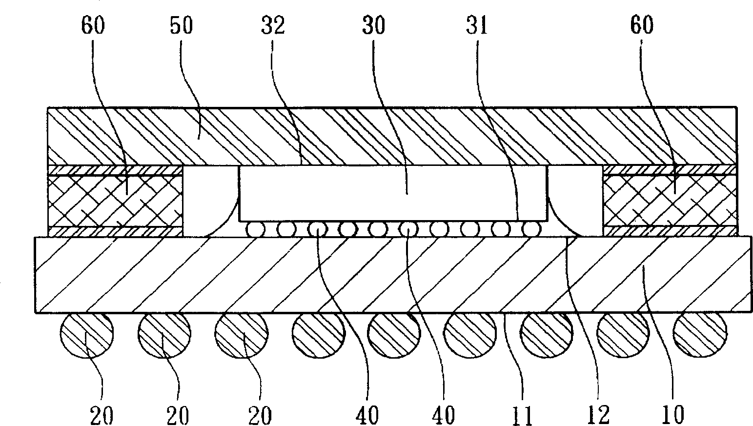
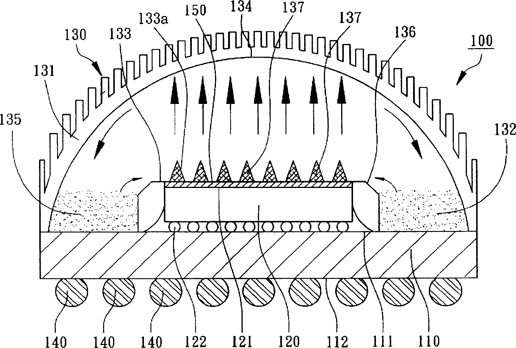
[0049] see figure 2 Shown is a first embodiment of the heat dissipation flip chip package structure of the present invention. The heat dissipation flip chip package structure 100 includes a substrate 110 , a flip chip 120 and a heat sink 130 . The substrate 110 has an upper surface 111 . In this embodiment, the heat dissipation flip chip package structure 100 includes a plurality of solder balls 140 disposed on the lower surface 112 of the substrate 110 . The flip chip 120 is bonded to the upper surface 111 of the substrate 110 , and the flip chip 120 has a back surface 121 . In this embodiment, the flip chip 120 is electrically connected to the substrate 110 through a plurality of bumps 122 .

[0050] The radiator 130 is arranged on the back surface 121 of the flip chip 120, wherein the radiator 130 includes a heat dissipation shell 131 and a coolant 132, the heat dissipation shell 131 is a closed space, and includes a bottom heat exchange part 133, A top heat exchange pa...


PUM


Abstract

The capsulation structure includes a base plate with an up surface, a wafer of composite crystal jointed to the up surface, and a radiator setup on back face of the wafer. The radiator includes a shell body for heat elimination and refrigerant. The shell body for heat elimination possesses a bottom heat exchanger, top heat exchanger and a part for collecting refrigerant. Including multiple heat radiating convex poles, the bottom heat exchanger is in use for increasing area of dissipation. The part for collecting refrigerant is connected to the bottom heat exchanger and the top heat exchanger. When carrying out thermolysis circulation inside the shell body, refrigerant can flow to heat radiating convex poles to be vaporized. The shell body for heat elimination and the refrigerant are in use for promoting efficiency of heat conduction of the capsulation structure in order to maintain normal temperature.

Description

technical field [0001] The present invention relates to a heat dissipation flip chip package structure, in particular to a heat dissipation flip chip package structure with a heat sink. Background technique [0002] Since today's electronic products emphasize high functionality and extremely high performance, the chips of these electronic products are in a high-computing state for a long time, which will cause a large amount of heat energy to be generated by the chip. If it is emitted, it will easily cause the chip to warp or crack, which will cause these electronic products to fail or be scrapped, thereby reducing the lifespan of the product. Therefore, today's highly computing chips are equipped with heat dissipation Installed on a non-active surface of the chip to speed up the dissipation of heat energy. [0003] see figure 1 Shown is a conventional heat dissipation package structure, which includes a substrate 10 , a plurality of solder balls 20 , a flip chip 30 , a pl...

Claims


Application Information

Patent Timeline
Patent Type & Authority Applications(China)
IPC IPC(8): H01L23/34H01L23/367H01L23/427
CPCH01L2224/16225H01L2224/73204H01L2224/73253H01L2924/15311
Inventor 刘安鸿赵永清李耀荣
Owner CHIPMOS TECH INC
Why Eureka
Try Eureka