Minisized imaging lens
A lens and miniature technology, applied in the direction of optical components, optics, instruments, etc., can solve the problems of long overall length, loss of competitiveness, and heavy weight of the lens, and achieve the effect of low tolerance sensitivity, reduced tolerance sensitivity, and compact structure
- Summary
- Abstract
- Description
- Claims
- Application Information
AI Technical Summary
Problems solved by technology
Method used
Image
Examples
Embodiment Construction
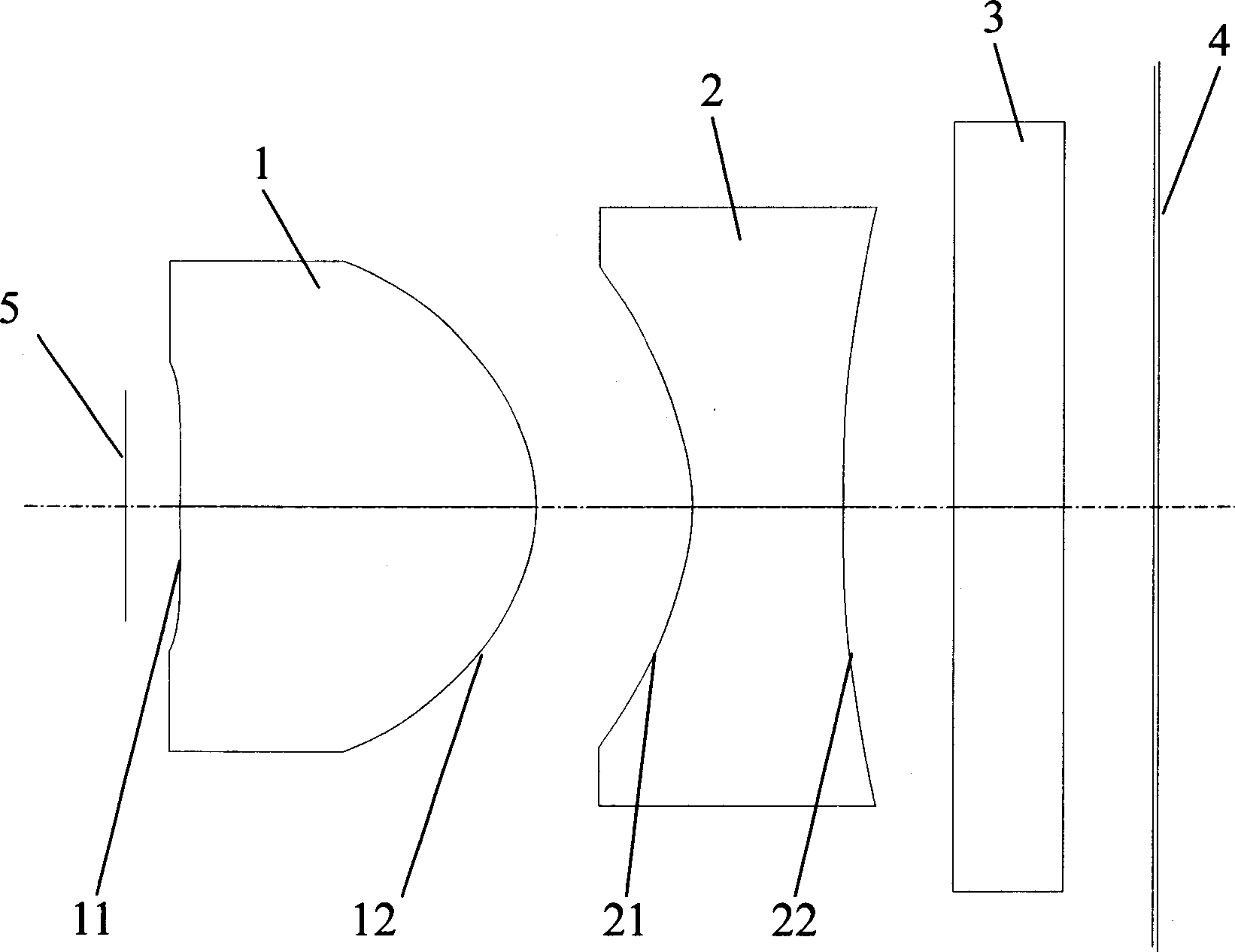
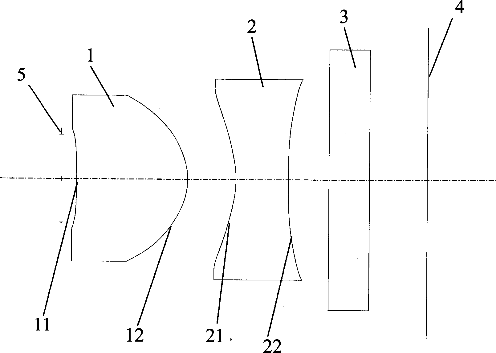
[0030] Such as figure 1 Shown is the optical structure diagram of the micro imaging lens of the present invention, the micro imaging lens includes a first lens 1 with a positive diopter and a second lens 2 with a negative diopter in order from the object side to the image side, so that light can pass through the first lens After the lens 1 and the second lens 2, focus on a CCD (Charge Coupled Device, Charge Coupled Device) or CMOS (Complementary Metal Oxide Semiconductor, Complementary Metal Oxide Semiconductor) image sensor 4 (imaging surface) to obtain a clear image . Wherein, the first lens 1 includes a first surface 11 facing the subject and a second surface 12 facing the imaging surface, the first surface 11 is a concave surface in a concave configuration relative to the subject, and the second surface 12 is a convex surface in a convex configuration relative to the imaging surface, so that the first lens 1 is in a half-moon shape, and at least one of the first and secon...
PUM
 Abstract
Description
Claims
Application Information
 - R&D
- Intellectual Property
- Life Sciences
- Materials
- Tech Scout
- Unparalleled Data Quality
- Higher Quality Content
- 60% Fewer Hallucinations
Browse by: Latest US Patents, China's latest patents, Technical Efficacy Thesaurus, Application Domain, Technology Topic, Popular Technical Reports.
© 2025 PatSnap. All rights reserved.Legal|Privacy policy|Modern Slavery Act Transparency Statement|Sitemap|About US| Contact US: help@patsnap.com


