Single-modulation-zone controlled 3X3 multi-mode interference type photoswitch
A multi-mode interference and optical switching technology, applied in the coupling of optical waveguides, can solve the problems of increasing switching loss and crosstalk, increasing the number of modulation areas, prolonging switching time, etc., achieving fewer control electrodes, simple modulation, and The effect of many channels
- Summary
- Abstract
- Description
- Claims
- Application Information
AI Technical Summary
Problems solved by technology
Method used
Image
Examples
Embodiment 1
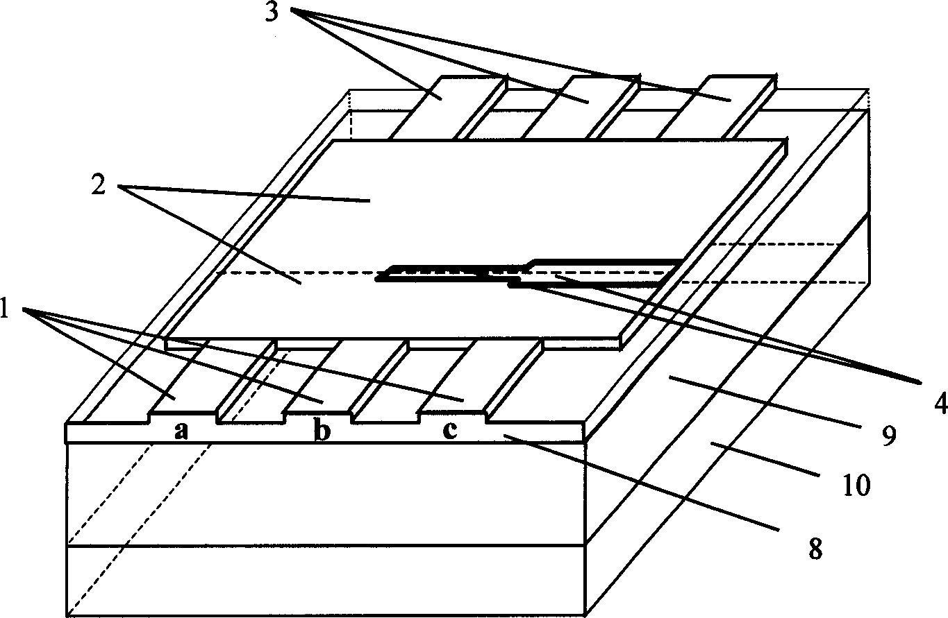
[0029] Such as image 3 As shown, the present invention includes a substrate substrate 10, a lower confinement layer 9 and a core layer; the core layer is composed of three input waveguides 1, a multimode waveguide region 2 and three output waveguides 3 connected in series; a single modulation region 4 is located on multimode waveguide zone 2.
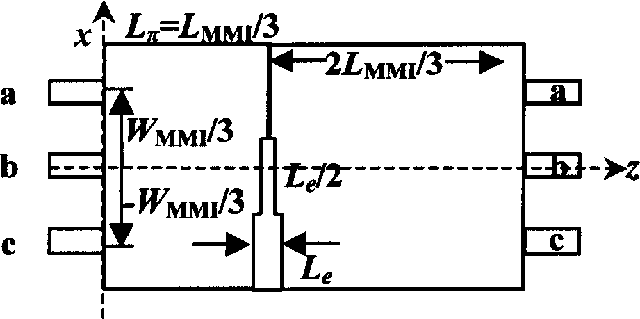
[0030] The single modulation area 4 is located at 1 / 3 or 2 / 3 of the longitudinal length of the multimode waveguide area 2, covering adjacent overlapping imaging image points, and the single modulation area 4 has a doubling relationship to the phases of these two image point modulations .
[0031] The single modulation area 4 uses multiple physical effects of materials to modulate the phase, such as light injection effect, thermo-optic effect, electro-optic effect or carrier injection effect. Different modulation methods and physical effects and the appearance of obvious images at image points The length of the difference determines t...
Embodiment 2
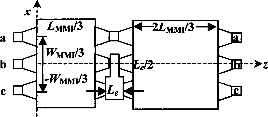
[0034] Such as Figure 4 As shown, the present invention includes a substrate substrate 10, a lower confinement layer 9 and a core layer; the core layer is composed of three input waveguides 1, two multimode waveguide regions 2, 5, three connecting waveguides 6, and a tapered transition The waveguide 7 is composed of three output waveguides 3 and a single modulation area 4; the input end of the first multimode waveguide 2 is connected to three input waveguides 1 through respective tapered waveguides 7, and the three connecting waveguides 6 are respectively connected through tapered waveguides 7 at both ends The output end of the first multimode waveguide 2 is connected with the input end of the second multimode waveguide 5, and the three output waveguides 3 at the output end of the second multimode waveguide 5 are connected with the output waveguides 3 through respective tapered waveguides, and in the three A single modulation area 4 is formed by connecting two adjacent wavegu...
PUM
 Abstract
Description
Claims
Application Information
 - R&D
- Intellectual Property
- Life Sciences
- Materials
- Tech Scout
- Unparalleled Data Quality
- Higher Quality Content
- 60% Fewer Hallucinations
Browse by: Latest US Patents, China's latest patents, Technical Efficacy Thesaurus, Application Domain, Technology Topic, Popular Technical Reports.
© 2025 PatSnap. All rights reserved.Legal|Privacy policy|Modern Slavery Act Transparency Statement|Sitemap|About US| Contact US: help@patsnap.com


