
Femtosecond electronic diffraction device

An electron diffraction and femtosecond technology, which is applied in the field of femtosecond electron diffraction devices, can solve the problems of reducing time resolution and achieve the effects of reducing time dispersion, high spatial resolution, and reducing movement distance

Inactive Publication Date: 2006-10-25
INST OF PHYSICS - CHINESE ACAD OF SCI
View PDF0 Cites 26 Cited by
  • Summary
  • Abstract
  • Description
  • Claims
  • Application Information

AI Technical Summary

Problems solved by technology

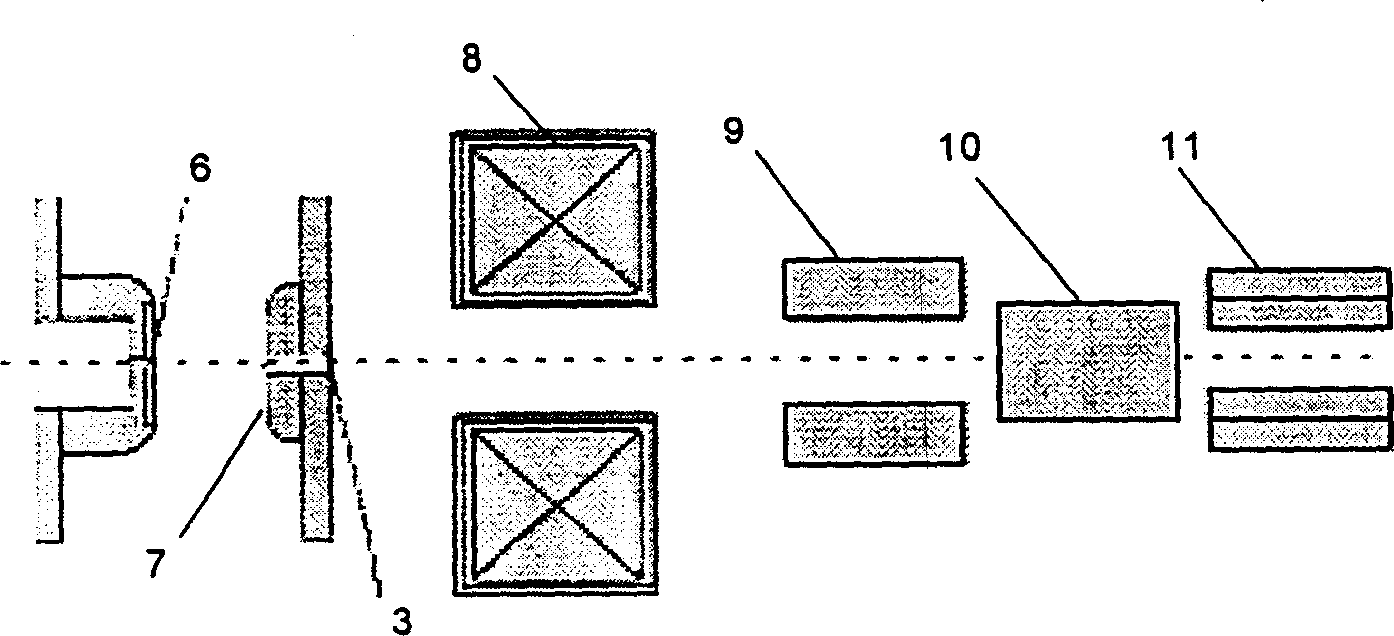
But the deficiency of this set of devices is that: if figure 1 As shown, after the electron beam is generated from the photocathode 6, it must pass through the anode 7, the magnetic lens 8, the X-direction deflection plate 9, the Y-direction deflection plate 10, and the scanning plate 11 to reach the sample. During this process, the electron beam has experienced a long movement distance; and because the electron beam has a space charge effect, the pulse width of such a long-distance moving electron beam will be correspondingly widened, thereby reducing the time resolution capability

Method used


Image

  • Femtosecond electronic diffraction device
  • Femtosecond electronic diffraction device
  • Femtosecond electronic diffraction device

Examples


Embodiment Construction

[0034] Below in conjunction with accompanying drawing and specific embodiment the present invention is described in further detail:

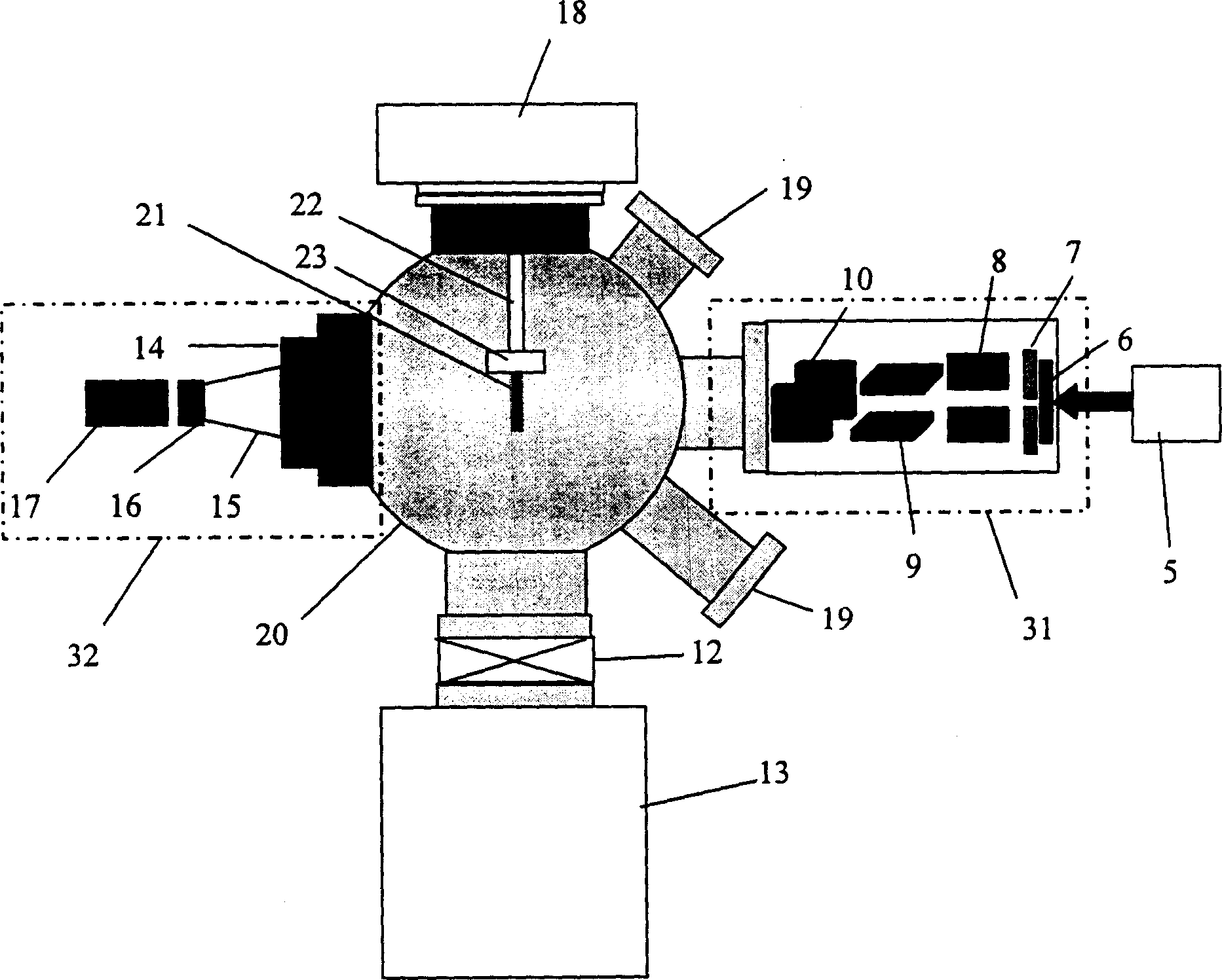
[0035] Such as figure 2 As shown, a femtosecond electron diffraction device includes a light source 5, an electron generation and control system 31, a sample chamber 20, an electronic measurement and imaging system 32, a vacuum system 13 and a five-axis control system 18; wherein:

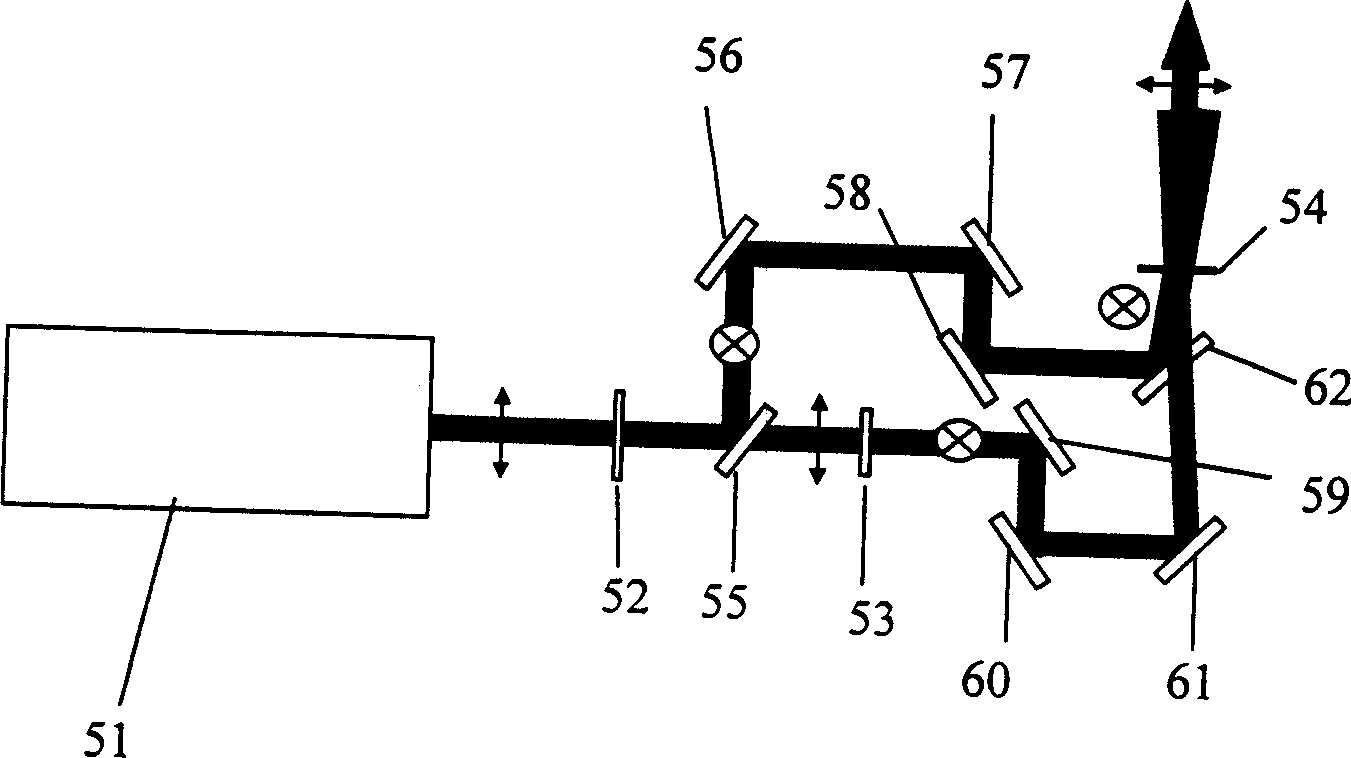
[0036] Such as image 3As shown, the light source 5 is a femtosecond Ti:Sapphire laser triple frequency generating device, and its realization is as follows: the pulse width of the output laser from the femtosecond Ti:Sapphire laser 51 is 30 femtoseconds, and the center wavelength is 800nm. 52. The cutting angle of the BBO frequency-doubling crystal is θ=29.2°, φ=0°, and the laser beam is split by the first dichroic beam splitter 55, which is completely transparent to the wavelength of 800nm ​​and completely reversed to the wavelength of 400nm; the frequency-doubli...


PUM

PropertyMeasurementUnit
Diameteraaaaaaaaaa
Thicknessaaaaaaaaaa

Abstract

The invention discloses a femtosecond electron diffraction device that includes light resource, electron generate and control system, sample room, electron measuring and imaging system, vacuum system and five shafts control system. The electron generating and controlling system includes photo cathode, anode, magnetic lens, X direction deflecting plate and Y direction deflecting plate. The invention decreases the distance from the cathode to sample and improves the time resolving power. The invention could be used to measure the structure dynamic information of transmission diffraction and reflection diffraction of the sample.

Description

technical field [0001] The invention relates to an electron diffraction device, in particular to a femtosecond electron diffraction device. Background technique [0002] In the research of laser technology, the appearance of femtosecond laser provides a powerful tool for scientists to study the ultrafast process of matter movement. However, the wavelength of the laser is too long, generally greater than 200nm, so the spatial resolution is far from enough to study the motion of matter. In order to obtain information with high spatial resolution, electrons and X-rays are generally used as detection means. At present, the technology that can be used as a femtosecond laser is very mature, and the titanium sapphire laser can obtain several femtosecond laser pulses. Time-resolved techniques are an important way to understand dynamic processes. In recent years, the optical pumping-electron beam detection method has provided an important experimental method for scientific researc...

Claims


Application Information

Patent Timeline
IPC IPC(8): G01N23/20H01J29/58H01J49/08
Inventor 张杰刘运全梁文锡
Owner INST OF PHYSICS - CHINESE ACAD OF SCI
Learn More