Electronic assembly wire and flat cable comprising same
A technology of electronic components and flat cables, which is applied in the field of wires and flat cables for electronic components, can solve the problems of preventing whiskers, insufficient, high cost, etc., and achieve the effect of preventing and suppressing whiskers
- Summary
- Abstract
- Description
- Claims
- Application Information
AI Technical Summary
Problems solved by technology
Method used
Image
Examples
Embodiment 1
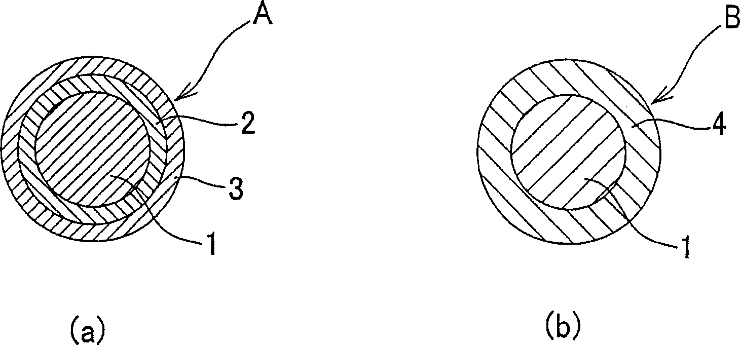
[0035] After pretreatment such as electrolytic degreasing and pickling, the copper wire (conductive substrate) with a diameter of 0.6 mm is subjected to Sn Bi alloy plating using plating chemicals produced by Ishihara Pharmaceutical Co., Ltd. (Japanese name: Ishihara Pharmaceutical Co., Ltd.) to form a Sn alloy plating layer (bottom plating).
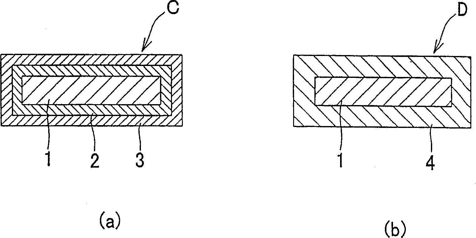
[0036] Next, Zn electroplating is performed to form an upper layer plating layer, and a lead wire having a double-layer structure plating layer is formed. Moreover, the stretching calender produced by SAIKAWA Corporation (Japanese name: サイカワ) performs stretching, calendering, and electrification annealing to make flat cables.
Embodiment 2
[0038] After carrying out electrolytic degreasing, pickling and other pretreatments to the copper wire (conductive substrate) with a diameter of 0.6 mm, Sn Zn alloy electroplating is carried out using electroplating chemicals produced by Nippon Metal Plating Co., Ltd. A Sn alloy plating layer (underlayer plating layer) is formed.
[0039] Next, Zn electroplating is performed to form an upper layer plating layer, and a lead wire having a double-layer structure plating layer is formed. Then, stretching, rolling, and electrical annealing were performed by the above-mentioned stretching calender to produce a flat cable.
Embodiment 3
[0041] After pretreatments such as electrolytic degreasing and pickling, the copper wire (conductive substrate) with a diameter of 0.6mm is subjected to Sn Cu alloy plating using a plating solution produced by Uemura Industry Co., Ltd. (Japanese name: Uemura Industry) to form a Sn alloy plating layer (bottom plating).
[0042] Next, Zn electroplating is performed to form an upper layer plating layer, and a lead wire having a double-layer structure plating layer is formed. Then, stretching, rolling, and electrical annealing were performed by the above-mentioned stretching calender to produce a flat cable.
PUM
 Abstract
Description
Claims
Application Information
 - R&D Engineer
- R&D Manager
- IP Professional
- Industry Leading Data Capabilities
- Powerful AI technology
- Patent DNA Extraction
Browse by: Latest US Patents, China's latest patents, Technical Efficacy Thesaurus, Application Domain, Technology Topic, Popular Technical Reports.
© 2024 PatSnap. All rights reserved.Legal|Privacy policy|Modern Slavery Act Transparency Statement|Sitemap|About US| Contact US: help@patsnap.com


