Monitoring marking layout for microlens baking process

A technology of micro-lens and marking, which is applied in the direction of lens, exposure device of photo-plate making process, exposure equipment of micro-lithography, etc. It can solve the problems of difficult reflective pattern, poor efficiency, large error, etc.

Active Publication Date: 2006-09-27
UNITED MICROELECTRONICS CORP
View PDF0 Cites 0 Cited by
  • Summary
  • Abstract
  • Description
  • Claims
  • Application Information

AI Technical Summary

Problems solved by technology

However, this method is not only inefficient, but also as the thickness of the microlens gradually shrinks, it becomes more and more difficult to distinguish the reflective pattern with the naked eye, and the error is also greater
In addition, the current technology cannot evaluate the flow of the photoresist after baking and the quality of the microlens array

Method used


Image

  • Monitoring marking layout for microlens baking process
  • Monitoring marking layout for microlens baking process
  • Monitoring marking layout for microlens baking process

Examples


Embodiment Construction

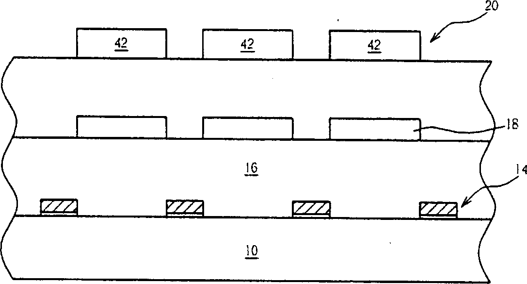
[0032] see Figure 5 , which shows the layout of the monitoring marks and the top view of the microlens array that can be used to check the baked state of the microlens in the preferred implementation of the present invention. Such as Figure 5 As shown, the microlens array 20 is formed in the active circuit area 101 with a plurality of unbaked photoresist blocks 42 . In the present invention, the monitoring mark layout 100 for checking the baked state of the microlens can be formed in the scribe area 102 and defined simultaneously with the photoresist block 42 . The size of the layout shown in the figure is for reference only.

[0033] According to this preferred embodiment, the monitoring mark layout 100 for checking the baked state of the microlens can be a U-shaped pattern, including two vertical line patterns 110 and 120 arranged in parallel to each other, and a horizontal line pattern 130 connecting the aforementioned two vertical lines. Line patterns 110 and 120 . Th...


PUM


Abstract

This invention relates to a monitoring marking layout for microlens baking process. Wherein, it comprises: two vertical-line pattern paralleled with each other, and one horizontal-line pattern connected to the vertical to define a pointer path and fluidize the vertical pattern to lead the horizontal pattern fusing along the path and forming design; then, uses the design to decide whether there once a roasting process to the microlens.

Description

technical field [0001] The invention relates to the manufacture of microlenses, in particular to a monitoring mark for the baking process of the microlenses, which is made on the cutting line and can be used to evaluate whether the microlens array has been baked and the quality of the baking. Background technique [0002] As known to those in the industry, microlens technology has been widely used in many optoelectronic products currently on the market, such as digital cameras and digital video cameras. The purpose of using the microlens is to control the direction of the light, so that the light can be gathered in the sensing area of ​​the light sensing chip. [0003] A digital camera usually includes a stacked color filter array (CFA) and a charge-coupled device (CCD) or complementary metal oxide semiconductor (CMOS) image sensor, wherein the color filter array includes three (R / G / B) or above staggered filter channels, each filter channel only allows light of a specific ...

Claims


Application Information

Patent Timeline
IPC IPC(8): G02B3/00G03F7/20
Inventor 刘恩廷陈建豪林欣蔚周德瑜
Owner UNITED MICROELECTRONICS CORP
Why Eureka
Try Eureka