


Quick Research
Generate reliable direction feasibility study reports for your R&D in just a few steps.

Technical Q&A
Discover and master advanced knowledge NOW. Basics, ideas, possibilities, all at once.

Find Solutions
As an expert in R&D theories, this can generate solutions to your technical problems instantly.

Evaluate Feasibility
Analyze your overall solution with one click, know your potential R&D risks in advance.

Monitor Landscape
Get weekly tech updates, stay abreast of the latest tech innovations and key insights.
Semiconductor device
A semiconductor and device technology, applied in the field of semiconductor devices, can solve the problems of deformation of semiconductor elements 3, difficulty in structural design, and low connection height of connecting terminals 4, so as to suppress deformation of connecting parts, improve structural design freedom, and reduce connection stress Effect
- Summary
- Abstract
- Description
- Claims
- Application Information
AI Technical Summary
Problems solved by technology
Method used
Image

Examples
Embodiment approach 1
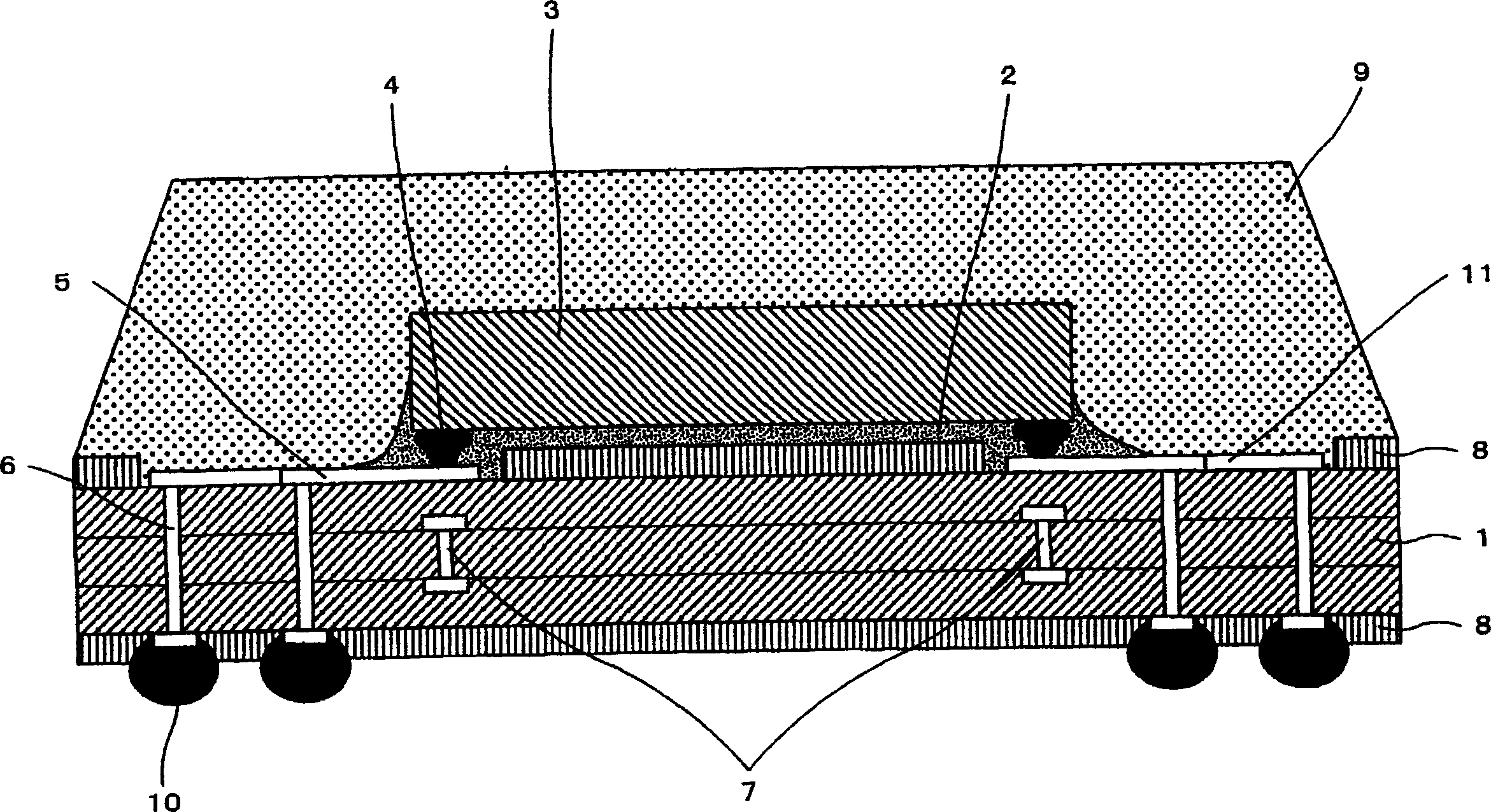
[0028] figure 1 It is a cross-sectional view showing the structure of the semiconductor device according to Embodiment 1 of the present invention.
[0029] Such as figure 1 As shown, a wiring circuit 11 including a connection electrode 5 and a resist 8 are disposed on one main surface of a substrate 1 . The resist may cover the wiring circuit 11 other than the connection electrode 5 or may expose the wiring circuit 11 . It is preferable to form the resist 8 on the wiring circuit 11 with such a thickness that there is no fear of pinholes in the resist 8, specifically 10 μm. A semiconductor element 3 having connection terminals 4 is mounted face down on the substrate 1 . The installation method is carried out by the following assembly method. That is, the semiconductor element 3 having the connection terminals 4 connected to the pads on the semiconductor element 3 is faced downward by a wire bonding device, and while heating, the substrate 1 is pressed with a pressure of 2...
Embodiment approach 2
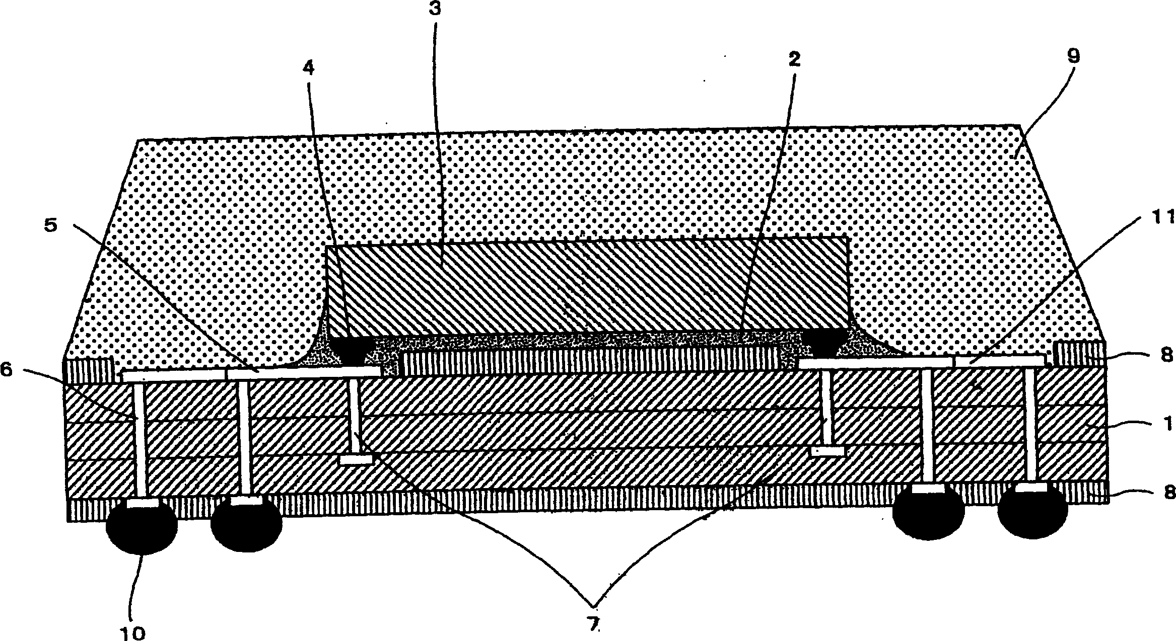
[0038] figure 2 It is a cross-sectional view showing the structure of the semiconductor device according to Embodiment 2 of the present invention.
[0039] The second embodiment has a structure in which the reinforcement via 7 extends to the lower surface of the connection electrode 4 and does not reach the other main surface side of the substrate 1 in the semiconductor device of the first embodiment.
[0040] Such as figure 2 As shown, a wiring circuit 11 including a connection electrode 5 and a resist 8 are disposed on one main surface of a substrate 1 . The resist may cover the wiring circuit 11 other than the connection electrode 5 or may expose the wiring circuit 11 . It is preferable to form the resist 8 on the wiring circuit 11 with such a thickness that there is no fear of pinholes in the resist 8, specifically 10 μm. A semiconductor element 3 having connection terminals 4 is mounted face down on the substrate 1 . The installation method is the following assembly...
Embodiment approach 3
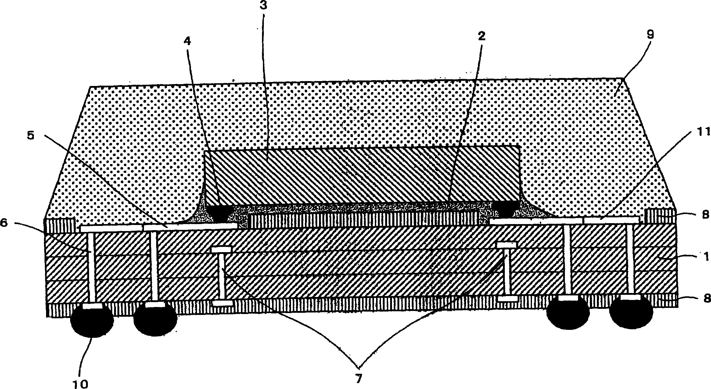
[0050] image 3 is a cross-sectional view showing the structure of the semiconductor device according to Embodiment 3 of the present invention.
[0051] This third embodiment has a structure in which the reinforcing via 7 is extended to the other main surface of the substrate 1 in the above-described first embodiment, and the reinforcing via 7 is electrically insulated from the connection electrode 5 .
[0052] Such as image 3 As shown, a wiring circuit 11 including a connection electrode 5 and a resist 8 are disposed on one main surface of a substrate 1 . The resist may cover the wiring circuit 11 other than the connection electrode 5 or may expose the wiring circuit 11 . It is preferable to form the resist 8 on the wiring circuit 11 with such a thickness that there is no fear of pinholes in the resist 8, specifically 10 μm. A semiconductor element 3 having connection terminals 4 is mounted face down on the substrate 1 . The installation method is carried out by the foll...
PUM
 Abstract
Description
Claims
Application Information
 - R&D Engineer
- R&D Manager
- IP Professional
- Industry Leading Data Capabilities
- Powerful AI technology
- Patent DNA Extraction
Browse by: Latest US Patents, China's latest patents, Technical Efficacy Thesaurus, Application Domain, Technology Topic, Popular Technical Reports.
© 2024 PatSnap. All rights reserved.Legal|Privacy policy|Modern Slavery Act Transparency Statement|Sitemap|About US| Contact US: help@patsnap.com