Method for producing static discharging protection in micro module and relative microelectronic module

A technology of electrostatic discharge and microelectronics, applied in the direction of circuits, electrical components, electric solid devices, etc., can solve the problems of increasing the number of microelectronic module pads and increasing the demand for microelectronic module areas

Inactive Publication Date: 2006-01-04
INFINEON TECH AG
View PDF0 Cites 1 Cited by
  • Summary
  • Abstract
  • Description
  • Claims
  • Application Information

AI Technical Summary

Problems solved by technology

According to this method, a pad must be added to each independent voltage supply domain, resulting in the problem of increasing the number of pads in the microelectronic module
[0007] A third method implemented with a shared ground network provides coupling effects via diodes and very complex additional protection methods, the disadvantage of this method is that it increases the area requirements of the microelectronic module

Method used


Image

  • Method for producing static discharging protection in micro module and relative microelectronic module
  • Method for producing static discharging protection in micro module and relative microelectronic module

Examples


Embodiment Construction

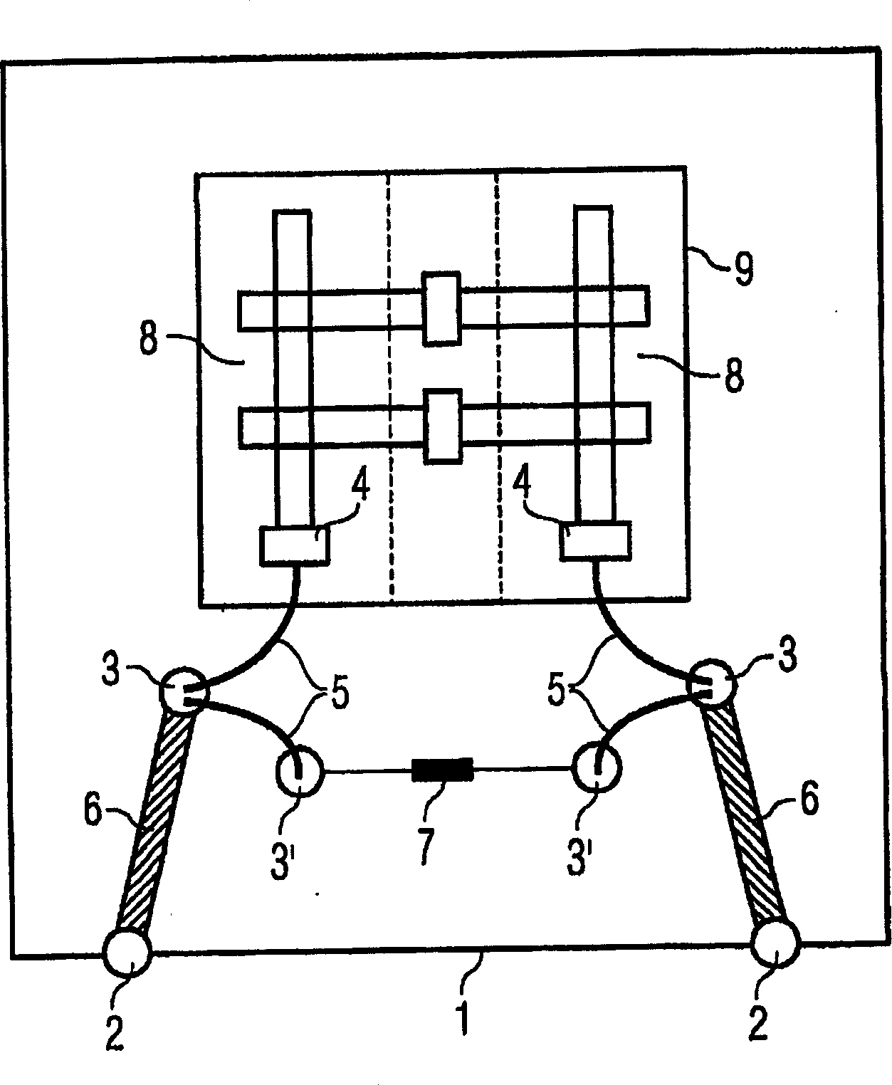
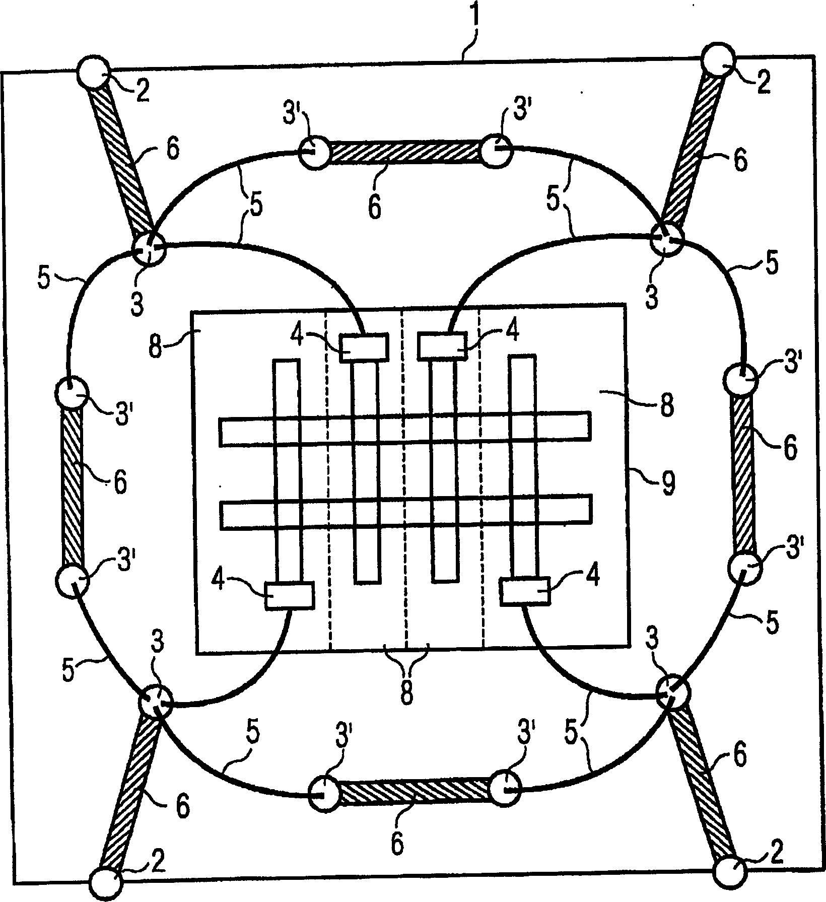
[0025] figure 1 Shown is a microelectronic module 1 comprising a semiconductor circuit 9 with two independent voltage supply domains 8 each having a voltage supply connection pad 4 connected via a connection line 5 to An internal terminal 3, (in another embodiment, the connection between the voltage supply connection pad 4 and the internal terminal 3 can also be realized only by a soldering point instead of the connecting line 5), each The internal terminal 3 is connected to an external terminal 2 of the microelectronic module 1 via an interconnection package 6 and to another internal terminal 3 ′ via a connecting line 5 . The two internal terminals 3' are connected to each other by means of an inducer 7, which can be achieved for example by coils, whereby a low-group resistive connection with a high inductance establishes a voltage supply connection between two independent voltage supply domains 8 between liner 4.

[0026] The ESD protection of the microelectronic module 1 ...


PUM


Abstract

A method of producing an electrostatic discharge (ESD) protection in a microelectronic module comprising a semiconductor circuit comprising at least two independent voltage supply domains each having at least one voltage supply connection pad , which are disclosed together with a corresponding microelectronic module. In this case, there is an electrical connection between two voltage supply link pads of two separate voltage supply domains, which is routed outside the semiconductor circuit and, for example, by a bonding wire or a solder joint And achieve.

Description

technical field [0001] The present invention relates to a method for generating ESD protection (protection against electrostatic discharge), and to a microelectronic module realized by the method. Background technique [0002] In the present case, the microelectronic module comprises a microelectronic circuit or a semiconductor circuit and a package which in particular comprises an interface of the microelectronic module to the outside world. [0003] A proper ESD protection of integrated circuits or microelectronic components requires low impedance current discharge paths. If the microelectronic module contains several independent voltage supply domains, according to the previous count, it is necessary to establish a low impedance electrical connection between these independent voltage supply domains, at least establish the ground supply or reference of each independent voltage supply domain. between potential supplies. This low-impedance electrical link, also known as gr...

Claims


Application Information

Patent Timeline
Patent Type & Authority Applications(China)
IPC IPC(8): H01L23/60
CPCH01L2224/49H01L2924/01013H01L2924/19107H01L2924/01005H01L2924/01033H01L23/60H01L24/48H01L23/50H01L2924/3011H01L2224/48091H01L2924/014H01L24/49H01L2224/16H01L2924/19105H01L2924/30107H01L2224/4911H01L2924/00014H01L2924/14H01L2224/05553H01L2924/10161H01L2224/45099H01L2224/05599H01L2924/00
Inventor P·佩斯F·泽恩格
Owner INFINEON TECH AG
Why Eureka
Try Eureka