Image sensor and method for fabricating the same

An image sensor and partial light technology, applied in solid image signal generators, image communication, image signal generators, etc., can solve the problems of high driving voltage, lack of color images, and high processing costs

Inactive Publication Date: 2005-11-16
DONGBUANAM SEMICON
View PDF0 Cites 5 Cited by
  • Summary
  • Abstract
  • Description
  • Claims
  • Application Information

AI Technical Summary

Problems solved by technology

However, the disadvantages of CCD are: high driving voltage is required, additional circuits are required, and processing costs are high
Therefore, the color image finally obtained by the interpolation circuit does not have the normal 1:1:1 ratio of red, green, and blue, resulting in low display quality in terms of color and resolution

Method used


Image

  • Image sensor and method for fabricating the same
  • Image sensor and method for fabricating the same
  • Image sensor and method for fabricating the same

Examples


Embodiment Construction

[0028] Preferred embodiments of the invention will now be described in detail, examples of which are illustrated in the accompanying drawings. Wherever possible, the same reference numbers will be used throughout the drawings to refer to the same or like parts.

[0029] Hereinafter, an image sensor and a manufacturing method thereof according to the present invention are described as follows.

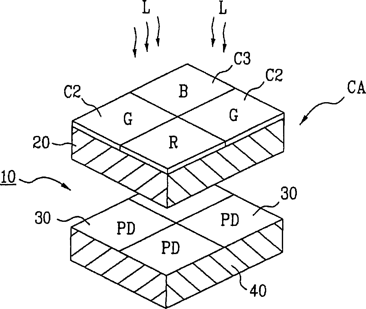
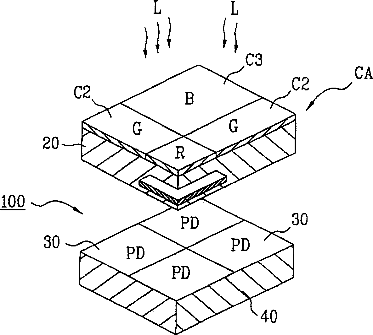
[0030] Such as image 3 As shown, the CMOS image sensor 100 of the present invention, that is, a CMOS image sensor for displaying a color image, includes a photodiode 30 formed on a semiconductor substrate 40 to generate and store a series of photocharges from external input light L, and a color filter array CA that colorizes externally input light and transmits the colored light to the photodiode 30 . In this case, the intermediate layer 20 is interposed between the color filter array CA and the photodiode 30 so as to transmit the light transmitted through the color filter array CA to...


PUM


Abstract

An image sensor and a method for fabricating the same are disclosed, in which a partial light-shielding layer is additionally arranged on a path of a particular colored light, for example, a red colored light that may cause excessive permeation, to partially shield the corresponding red colored light in a state that red colored light, green colored light and blue colored light are permeated into each photodiode of a semiconductor substrate, so that the permeation position of the red colored light coincides with that of the green colored light and the blue colored light each having the wavelength shorter than that of the red colored light, thereby normally generating optical charges caused by the red colored light in an effective depletion area of the photodiode like those caused by the green colored light and the blue colored light. The permeation position of a red colored light, a green colored light and a blue colored light coincides with one another within a depletion area of a semiconductor substrate to obtain an optimal effective ratio from respective optical charges and the uniform quantity of the respective optical charges can be transferred / discharged to an interpolation circuit by signal processing transistors, thereby effectively displaying color images having excellent display quality (in color and resolution) approximate to a ratio of 1:1:1 with red, green and blue.

Description

[0001] This application claims priority from Korean Patent Application No. P2003-101702 filed on December 31, 2003, which is incorporated herein by reference. technical field [0002] The present invention relates to an image sensor, and more particularly to an image sensor and a manufacturing method thereof, wherein a part of the light-shielding layer is additionally arranged on the path of light of a specific color (such as red light) that may cause excessive transmission, so as to partially shield the corresponding Red light, so that red light, green light and blue light penetrate each photodiode of the semiconductor substrate, so the transmission position of red light is consistent with the transmission position of green light and blue light, and the respective wavelengths of green light and blue light The wavelength of red light is shorter than that of red light, so that the photocharge due to red light is normally generated in the effective dissipation region of the photo...

Claims


Application Information

Patent Timeline
Patent Type & Authority Applications(China)
IPC IPC(8): H01L27/14H01L27/146H01L31/10H04N1/46H04N3/14H04N5/335H04N5/369H04N5/374H04N9/04
CPCH01L27/14621H01L27/14685H04N2209/045H04N9/045H01L27/14645H01L27/14623H01L27/146H01L31/10
Inventor 韩昌勋
Owner DONGBUANAM SEMICON
Why Eureka
Try Eureka