Dielectric waveguide filter

A waveguide filter, dielectric technology, applied in waveguide devices, waveguides, circuits, etc., can solve problems such as low yield and high variability

Inactive Publication Date: 2005-06-15
NEC CORP
View PDF0 Cites 6 Cited by
  • Summary
  • Abstract
  • Description
  • Claims
  • Application Information

AI Technical Summary

Problems solved by technology

As a result, problems such as high variability in performance and low yields were encountered in fabrication

Method used


Image

  • Dielectric waveguide filter
  • Dielectric waveguide filter
  • Dielectric waveguide filter

Examples


Embodiment Construction

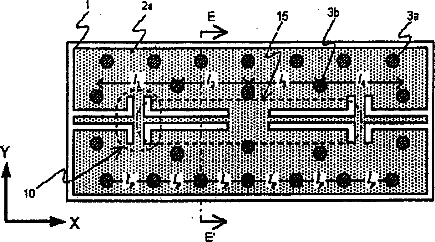
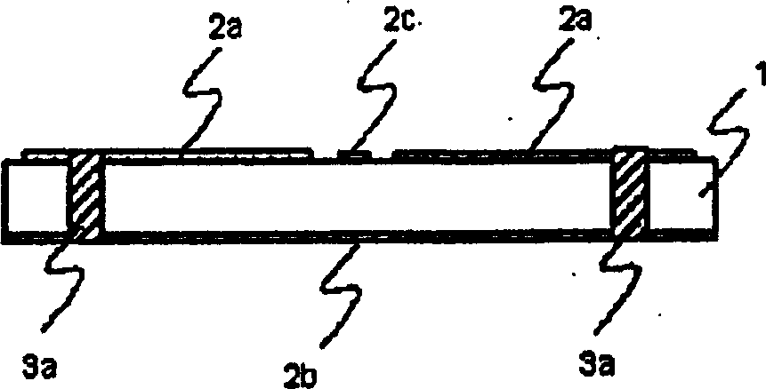
[0024] Referring now to FIG. 2, a first embodiment of the present invention will be described in detail. Figure 2A shows a plan view of the filter substrate, and Figure 2B shows along the Figure 2A The cross-sectional view of alternating long and short dashed lines A-A' in .

[0025] Upper and lower conductive layers 2 a and 2 b are formed on the upper and lower surfaces of the dielectric substrate 1 . The upper and lower conductive layers 2a and 2b are connected to each other through via holes 3a and 3b, thereby forming first-level, second-level, and third-level dielectric resonators 5a, 5b and 5c and input / output waveguide structures 4a and 4b, Wherein the through holes 3a and 3b are formed at an interval equal to or less than 1 / 2 of the wavelength in the dielectric substrate at the resonance frequency. The filter is configured so that the first-stage resonator 5a and the second-stage resonator 5b are coupled by an electromagnetic field by means of a dielectric window ...


PUM


Abstract

A conductive layer is formed on each of the upper and lower surfaces of the dielectric substrate, and the two conductive layers are connected through the formed via row, thereby forming an n-level dielectric resonator and an input / output waveguide structure, wherein the formed The spacing of the rows of vias is less than or equal to 1 / 2 of the wavelength in the dielectric substrate at the resonant frequency. If it is assumed that the number of stages n is 3, then the first-stage resonator and the second-stage resonator are coupled by the electromagnetic field relying on the through hole of the first interval; the second-stage resonator and the third-stage resonator are coupled by relying on the second interval The electromagnetic field of the through hole is coupled, thereby forming a filter. The input / output waveguide structure and the filter are coupled through the electromagnetic field by virtue of the fourth spaced vias. The first resonator and the third resonator are coupled by an electromagnetic field via the third spaced through holes.

Description

technical field [0001] The present invention relates to a dielectric waveguide filter having an upper conductive layer and a lower conductive layer on the surface of a dielectric substrate, wherein a row of vias or wires connecting the upper conductive layer and the lower conductive layer is used to form a resonator and a dielectric window. Background technique [0002] There is a need for filters characterized by low loss and steep out-of-band rejection characteristics, and further, by compact size and connectability to planar circuits. From the point of view of connection reproducibility and low parasitic inductance at high frequencies, it is also strongly desirable that the filter allows flip-chip packaging. Figure 1 shows a filter with these characteristics, and this filter is described in the published paper by M. Ito et al (IEEE International Microwave Symposium Digest, pp.1597-1600 May 2001). Figure 1A is a planar graph of known filter instances, and Figure 1B It i...

Claims


Application Information

Patent Timeline
Patent Type & Authority Applications(China)
IPC IPC(8): H01P1/208H01P5/107
CPCH01P1/2088H01P5/107
Inventor 伊东正治丸桥建一大畑惠一
Owner NEC CORP
Why Eureka
Try Eureka