
High destructive threshold value semiconductor saturable absorbing mirror for mode locked laser

A technology of saturable absorption and mode-locked lasers, which is applied in the field of semiconductor saturable absorption mirrors, can solve the problems of damage, low threshold of surface resistance to laser damage, etc., and achieve the effect of increasing reflectivity and improving the ability to resist laser damage

Inactive Publication Date: 2005-06-01
TIANJIN UNIV
View PDF0 Cites 5 Cited by
  • Summary
  • Abstract
  • Description
  • Claims
  • Application Information

AI Technical Summary

Problems solved by technology

However, the disadvantage of this design is that the surface has a low threshold of resistance to laser damage and is often damaged in use

Method used


Image

  • High destructive threshold value semiconductor saturable absorbing mirror for mode locked laser
  • High destructive threshold value semiconductor saturable absorbing mirror for mode locked laser

Examples


specific Embodiment approach

[0009] 1. Produce broadband or narrowband (visible light or near-infrared) semiconductor saturable absorption mirrors according to the manufacturing process. The specific implementation is as follows:

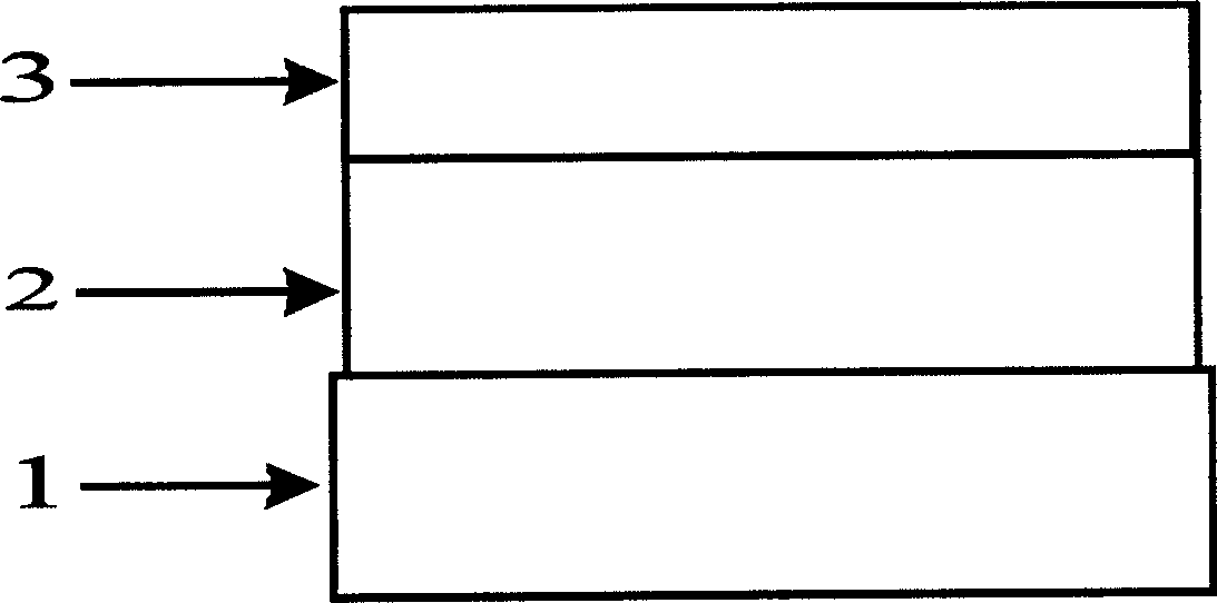
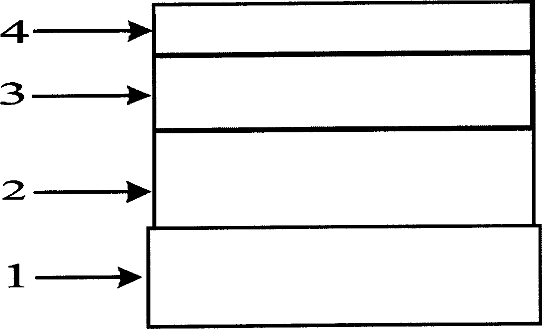
[0010] (a) Broadband semiconductor saturable absorption mirror: use MBE to press gallium arsenide stop layer and aluminum gallium arsenide stop layer, transparent semiconductor layer, semiconductor quantum well layer, transparent semiconductor layer, semiconductor quantum well on the surface of gallium arsenide substrate Layer and transparent semiconductor layer are grown sequentially, then a pair of high reflective films (composed of standard high and low refractive index dielectric film layers) are evaporated, then a transparent dielectric film is evaporated, and finally a metal reflective layer is deposited. The gold-plated side was bonded to a silicon semiconductor substrate as a base with epoxy resin. After mechanical grinding, solution etching and other procedures, the s...


PUM


Abstract

The present invention discloses one kind of saturable semiconductor absorbing mirror with high destruction threshold for mode locking laser, and belongs to the field of saturable absorbing mirror technology of mode locking laser. The saturable absorbing mirror includes silicon or Ga-As substrate, Bragg refection layer of metal film or Al-As / Ga-As, transparent Al-Ga-As or In-Al-Ga-As semiconductor layer, and saturable absorption layer of Ga-As or In-Ga-As quantum well. The present invention features that the surface of the saturable absorption layer has plated high reflectivity layer and the high reflectivity layer consists of at least three SiO2 film-ZrO2 film pairs in the optical thickness in one quarter of reflecting wavelength. The present invention has the obvious advantages of lowered transmitting light strength, raised capacity of resisting laser damage and the raised reflectivity of the mirror caused by the plated high reflectivity film.

Description

technical field [0001] The invention relates to a semiconductor saturable absorption mirror with a high destruction threshold of a mode-locked laser. It belongs to the saturable absorber mirror technology of mode-locked laser. Background technique [0002] A saturable absorber acts as a pure absorber for low-energy incident light, while for high-energy incident light, it becomes transparent due to the saturation of the absorption capacity. Such a substance is placed in the resonant cavity, and the loss of continuous light with small energy in the cavity increases, while the loss of high-energy pulses becomes smaller, so it plays a role in selecting and shaping the pulse and promotes pulse generation. It is an application in mode-locked lasers. of a technique. In the visible and near-infrared wavelength domains, suitable materials for fabricating saturable absorbers are semiconductors. The structure of the existing broadband semiconductor satu...

Claims


Application Information

Patent Timeline
Patent Type & Authority Applications(China)
IPC IPC(8): H01S3/02H01S3/098
Inventor 张志刚王勇刚柴路李建萍王清月
Owner TIANJIN UNIV
Learn More