Semiconductor device
A technology of semiconductors and conductors, applied in the field of semiconductor devices, can solve problems such as waveform distortion, adverse effects of signals, failure to adopt, etc., and achieve the effect of excellent electrical performance
- Summary
- Abstract
- Description
- Claims
- Application Information
AI Technical Summary
Problems solved by technology
Method used
Image

Examples
Embodiment 1
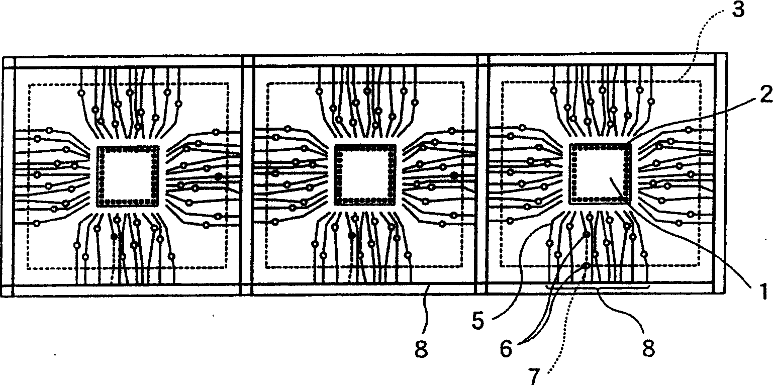
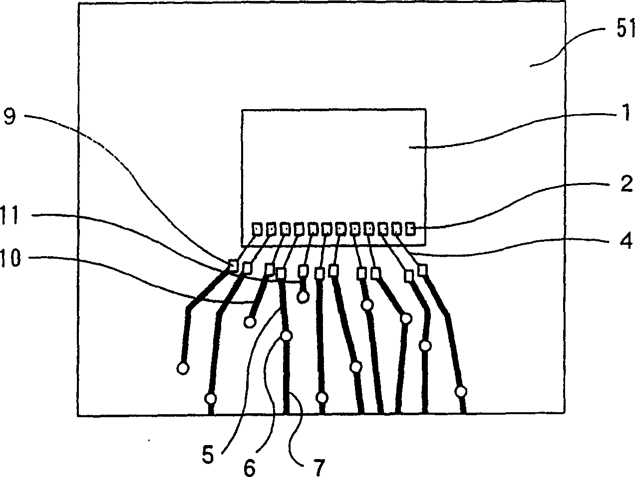
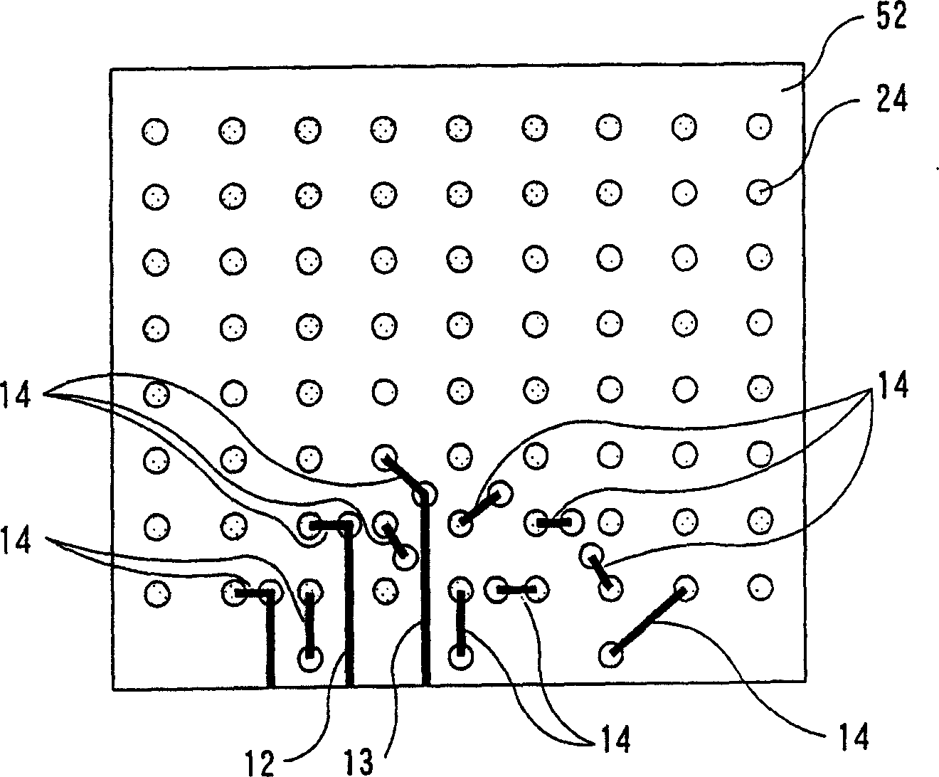
[0053] figure 1 is a plan view of a wiring substrate in Embodiment 1 of the semiconductor device of the present invention. Figure 2A for figure 1 A partial enlarged view of the semiconductor device, for the figure 1 An example of the pattern of the upper layer of the wiring substrate cut into a monolithic part, and is in figure 1 Among the four directions shown, only one direction is shown as a representative figure. Figure 2B Graphic example for the lower layer.
[0054] figure 1 Among them, a semiconductor element 1 has electrode terminals 2 . In this example, the semiconductor element 1 is mounted on a wiring board, but it shows a state that has not yet been encapsulated with resin. However, as in the above-mentioned known case, after packaging and mounting solder balls, it is finally cut along the cutting position 3 of each side shown by the dotted line.
[0055] exist Figure 2A and Figure 2B On the top, 51 is a wiring layer forming an upper layer, and 52...
Embodiment 2
[0063] Figure 5A and Figure 5B This is an example of a wiring pattern of a wiring substrate in Embodiment 2 of the semiconductor device of the present invention. The numbers in the figure are except conductor wiring 25, the rest and figure 1 , Figure 2A and Figure 2B The same as used in . The difference between Embodiment 2 and Embodiment 1 is that the conductor wiring, that is, the specific conductor wiring formed on a different wiring layer from the adjacent wire wiring, transmits a signal of ground or power. that is Figure 5A and Figure 5B , a specific conductor wiring 25 is connected to ground or a power supply.
[0064] According to the above structure, since the electroplating short wires 7 of the conductor wiring 25 of the grounding or power supply are at least on the different wiring layers 51, 52 from the electroplating short wires 12, 13 of the conductor wirings 10, 11 on both sides, the electroplating stub wires If they are not adjacent to each other,...
Embodiment 3
[0067] Figure 6 An example of a wiring pattern in Embodiment 3 of the semiconductor device of the present invention is shown. In addition to the conductor wiring 26, the numbers in the figure are the same as figure 1 , Figure 2A and Figure 2B The same as used in . The third embodiment differs from the first embodiment in that the transmission signal of the conductor wiring 26 is a digital signal.
[0068] According to the above structure, since the electroplating stub 7 of the conductor wiring 26 of the digital signal is at least on a different wiring layer from the electroplating stubs 12 and 13 (not shown) of the conductor wiring 10 and 11 on both sides, the two are not connected. Adjacent to each other, the distance between them increases, and the distance between the short wires for plating of the conductor wirings 10 and 11 and the conductor wiring 26 also increases.
[0069] Digital signals contain high-order harmonic components, which actually contain several t...
PUM
 Abstract
Description
Claims
Application Information
 - R&D
- Intellectual Property
- Life Sciences
- Materials
- Tech Scout
- Unparalleled Data Quality
- Higher Quality Content
- 60% Fewer Hallucinations
Browse by: Latest US Patents, China's latest patents, Technical Efficacy Thesaurus, Application Domain, Technology Topic, Popular Technical Reports.
© 2025 PatSnap. All rights reserved.Legal|Privacy policy|Modern Slavery Act Transparency Statement|Sitemap|About US| Contact US: help@patsnap.com