Double-face flip chip film

A chip-on-chip, double-sided technology, applied in the direction of electrical components, electric solid devices, circuits, etc., can solve the problems of reduced bending times, difficult assembly, poor reliability, etc., to improve reliability and increase the number of bending times , the effect of increasing ease

Inactive Publication Date: 2005-01-19
TPO DISPLAY
View PDF0 Cites 0 Cited by
  • Summary
  • Abstract
  • Description
  • Claims
  • Application Information

AI Technical Summary

Problems solved by technology

[0006] However, since the thickness of this double-sided chip-on-chip film is thicker than that of a single-sided chip-on-chip film, its elasticity is greater than that of a single-sided chip-on-chip film, which makes assembly difficult.
Moreover, because the thickness is thick, the number of bending times will be reduced, which in turn will deteriorate the reliability

Method used


Image

  • Double-face flip chip film
  • Double-face flip chip film
  • Double-face flip chip film

Examples


Embodiment Construction

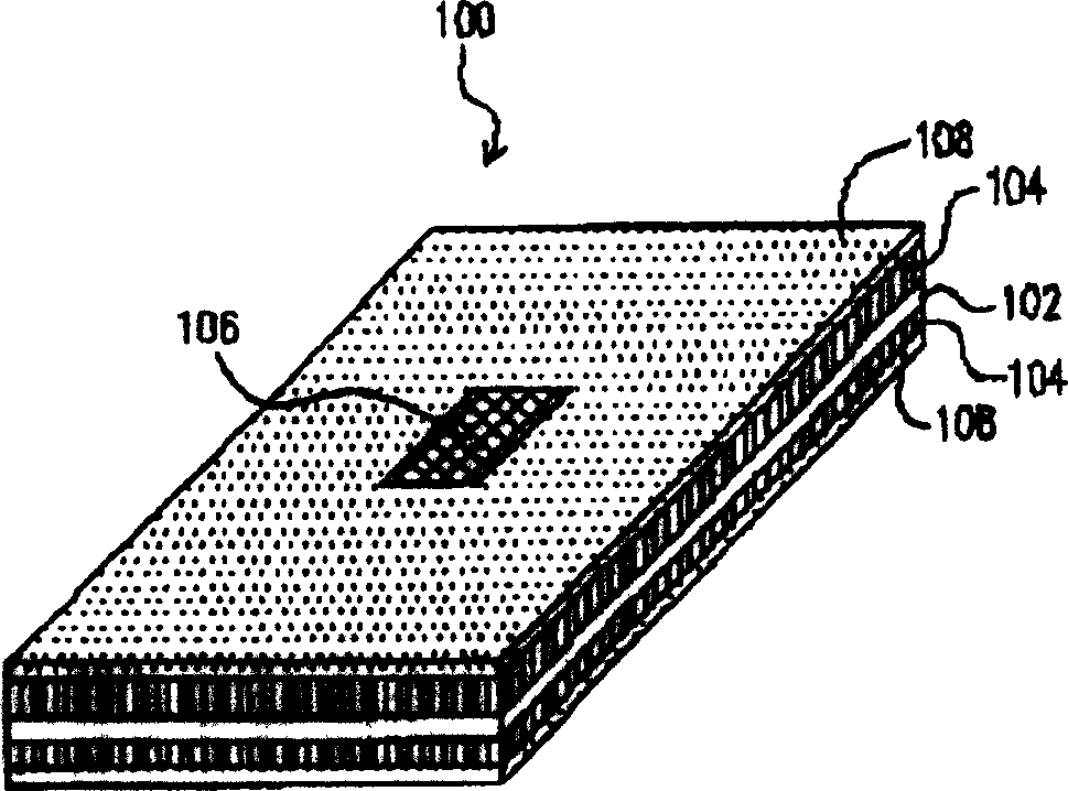
[0024] The double-sided chip-on-chip film of the present invention can be applied to various semiconductor elements or products, or applied to mobile phones and personal digital processors (PDAs), mainly in conjunction with the module packaging technology of liquid crystal displays (LCDs) therein. And the double-sided COF film of the preferred embodiment of the present invention is as Figure 2A and Figure 2B shown.

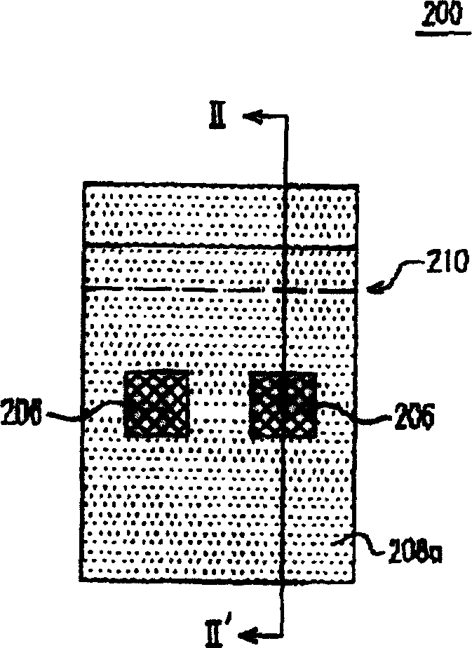
[0025] Figure 2A It is a schematic top view of a double-sided chip-on-chip film according to a preferred embodiment of the present invention, Figure 2B is Figure 2A The II-II′ section schematic diagram, please refer to Figure 2A and Figure 2B , the substrate 202 used in the double-sided chip-on-chip film 200 of the present invention is a flexible substrate, and its material can be selected from polyimide (Polyimide, PI), Teflon (Teflon), polyamide (Polyamide), polymethylmethacrylate (Polymethylmethacrylate), polycarbonate (Polycarbonate), polyester (P...


PUM


Abstract

The invention discloses a double-surface coated crystal film, at least composed of a flexible substrate, two conductor films situated on the right surface and at the back of the substrate and a covering layer on the conductor film. And it has a bending region for bending the bendable substrate, and the conductor film and covering layer cannot exist at the back of the substrate in the bending region. Because the double-surface film chip is designed by using the no-conductor film and covering-layer at the back of the substrate in the bending region, it can increase the number of bending times and bending easiness, and improve the convenience for mounting.

Description

technical field [0001] The present invention relates to a double-sided chip on film (COF for short), and in particular to a double-sided chip on film that can increase the number of bending times. Background technique [0002] The earliest packaging technology is the use of wire bonding packaging, that is, the use of printed circuit boards (Printed Circuit Board, referred to as PCB), but its disadvantages are high cost and large volume, so in recent years with the rise of portable electronic communications and information products, and semiconductors The demand for high-density IC packaging makes the use of flexible board packaging technology a major mainstream at present, such as chip scale packaging (Chip Scale Package, referred to as CSP) that uses flexible boards as substrates for carrying chips, or applications in mobile Telephones and Personal Digital Processors (PDAs). The FPC packaging technology first included Tape Automatic Bonding (TAB) technology, and then devel...

Claims


Application Information

Patent Timeline
IPC IPC(8): H01L23/12H01L23/48H01L23/50
Inventor 陈玉燮
Owner TPO DISPLAY
Why Eureka
Try Eureka