Semiconductor memory device having advanced data strobe circuit

A data strobe, pulse circuit technology, applied in digital memory information, information storage, static memory and other directions, can solve the problem of short timing margin, not suitable for high-speed operation and so on

Inactive Publication Date: 2004-12-01
SK HYNIX INC
View PDF0 Cites 2 Cited by
  • Summary
  • Abstract
  • Description
  • Claims
  • Application Information

AI Technical Summary

Problems solved by technology

Therefore, a shorter period of the external clock CLK, ie 1tCK, makes each alignment data have a shorter timing margin, ie 0.5tCK; so the data strobe circuit in the prior art is not suitable for semiconductor memory using high frequency High-speed operation of the device

Method used


Image

  • Semiconductor memory device having advanced data strobe circuit
  • Semiconductor memory device having advanced data strobe circuit
  • Semiconductor memory device having advanced data strobe circuit

Examples


Embodiment Construction

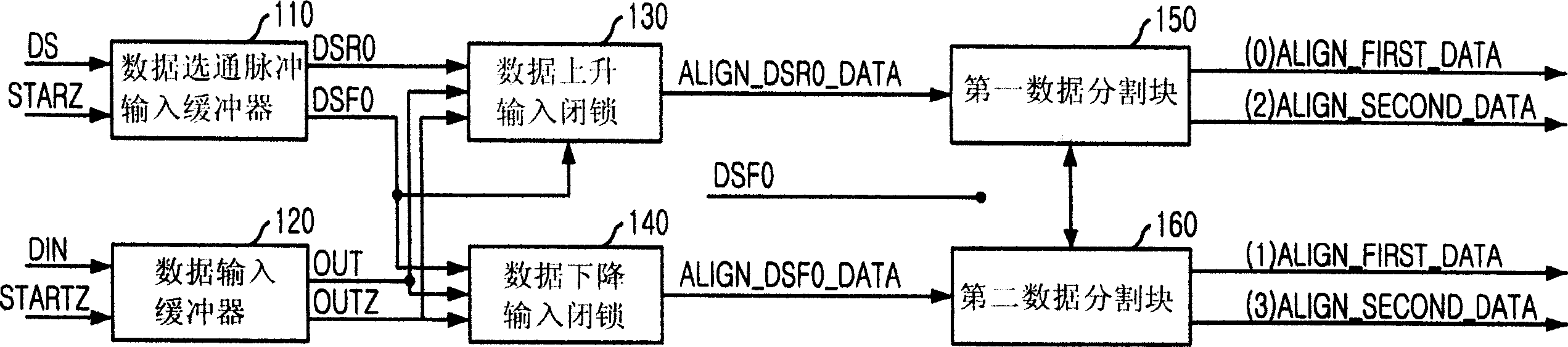
[0029] Hereinafter, a semiconductor memory device having an advanced data strobe circuit according to the present invention will be described in detail with reference to the accompanying drawings.

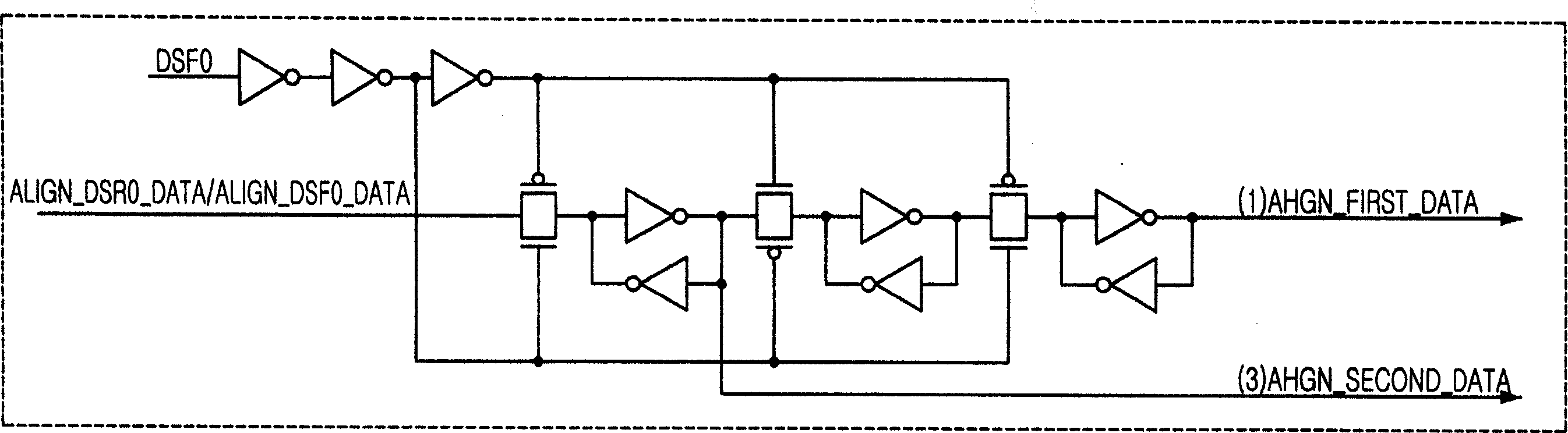
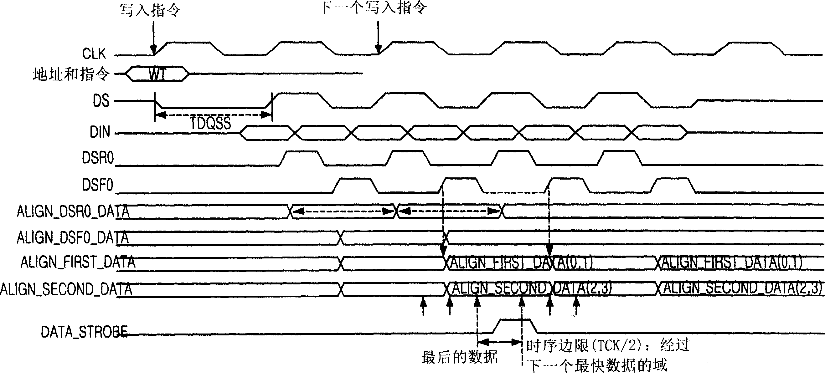
[0030] Figure 4 It is a block diagram of a data strobe circuit according to an embodiment of the present invention.

[0031] As shown in the figure, the data strobe circuit includes a data strobe buffer block 400, a data strobe division block 420, a data input buffer block 410, a blocking block with first to fourth blocking units 430 to 460, And a data alignment block having first to third alignment units 470 to 490.

[0032] The data strobe buffer block 400 receives the data strobe signal DS, and then outputs a buffered data strobe signal DSBUF_OUT. The data input buffer block 410 receives input data DIN, and then outputs buffered input data DIN_OUT. The data strobe splitting block 420 receives the buffered data strobe signal DSBUF_OUT, and then generates first rising and falli...


PUM


Abstract

A data strobe circuit for prefetching M number of N bit data, N and M being a positive integer, includes a data strobe buffering unit for generating N number of align control signals based on a data strobe signal; a synchronizing block having M number of latch blocks, each for receiving N bit data and outputting the N-1 bit data in a parallel fashion in response to N-1 number of the align control signals and one bit prefetched data in response to the remaining align control signals; and a output block having M number of aligning blocks, each for receiving the N-1 bit data in the parallel fashion, synchronizing the N-1 bit data with the align control signal and outputting the synchronized N-1 bit data as the N-1 bit prefetched data.

Description

technical field [0001] The present invention relates to a semiconductor memory device, in particular to a data strobe pulse circuit in the semiconductor memory device which has more time margins in data write operation. Background technique [0002] Generally, in double data rate synchronous dynamic random access memory (hereinafter referred to as DDR SDRAM), a method of prefetching 2-bit data or 4-bit data has been used to increase the operation speed of DDR SDRAM. However, since the time margin is small when DDR SDRAM prefetches individual bits of multi-bit data according to the prior art, some serious problems arise. Therefore, in order to increase the operation speed of DDR SDRAM, the method of prefetching multi-bit data is considered as a limiting condition. [0003] FIG. 1A is a block diagram of a data strobe circuit of a DDR SDRAM in the prior art, and FIG. 1B is a circuit diagram of a divided first / second data block 160 in the data strobe circuit of a DDR SDRAM in t...

Claims


Application Information

Patent Timeline
Patent Type & Authority Applications(China)
IPC IPC(8): G11C11/40G11C7/10G11C7/22G11C11/4076G11C11/4093
CPCG11C7/1072G11C7/1066G11C7/222G11C7/1087G11C7/1093G11C7/1078G11C7/1039G11C7/22G11C11/4093G11C11/4076G11C11/40
Inventor 权奇昌
Owner SK HYNIX INC
Why Eureka
Try Eureka