Opto-electronic device integration

A device and laser technology used in the field of integration of high-yield density integrated optoelectronic devices

Inactive Publication Date: 2004-08-18
CUFER ASSET LTD LLC
View PDF0 Cites 9 Cited by
  • Summary
  • Abstract
  • Description
  • Claims
  • Application Information

AI Technical Summary

Problems solved by technology

[0023] The prior art lacks a method to apply AR coatings on the entire wafer (i.e. lasers and detectors) without creating a patterned protective layer on the lasers

Method used


Image

  • Opto-electronic device integration
  • Opto-electronic device integration
  • Opto-electronic device integration

Examples


Embodiment Construction

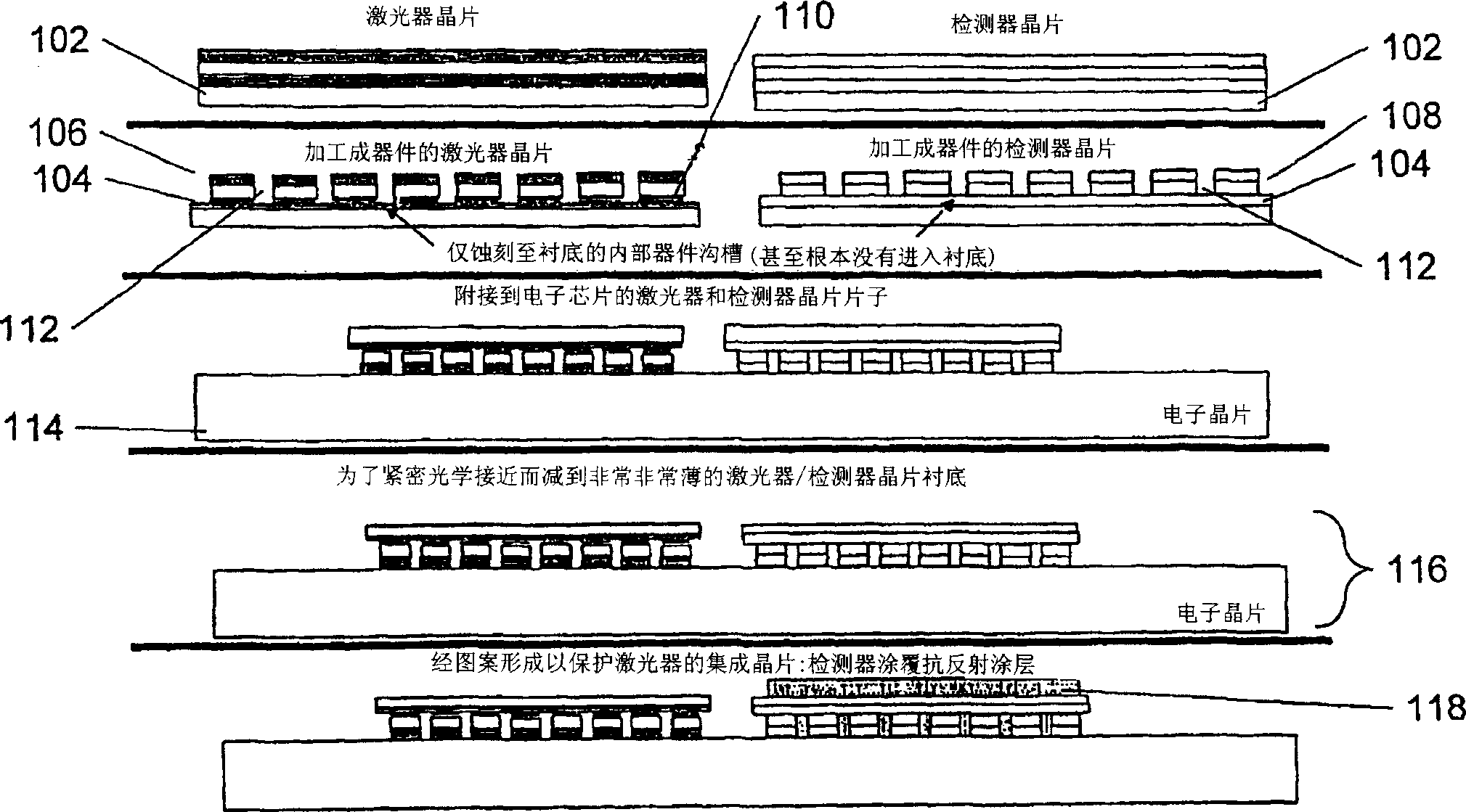
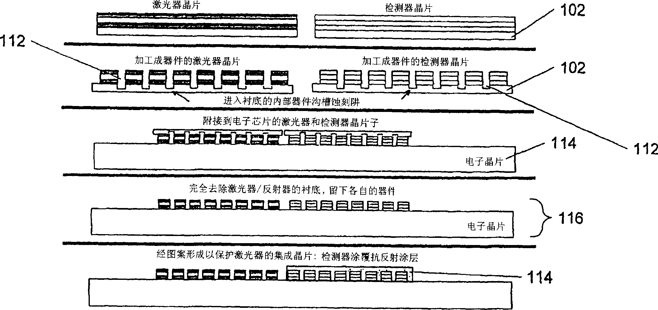
[0064] Figure 5 An exemplary method according to the teachings of the present invention is shown at a simplified high-level overview. This approach overcomes the shortcomings of previous approaches, while allowing optical access, removing absorbing regions, providing higher structural integrity, and having better heat dissipation properties.

[0065] exist Figure 5 A laser wafer 502 (consisting of lasers integrated on substrate 102) and a detector wafer 504 (consisting of lasers integrated on detector on the bottom 102). Alternatively, a hybrid wafer made of lasers and detectors integrated on a common substrate is fabricated or obtained eg in some alternate pattern or other combination.

[0066] The trenches 506 are etched to allow the wafer to be processed into individual devices (by etching the trenches into the substrate), or, in some cases, for example, as in a document entitled "Redundant Device Array" and contemporaneously herein As shown in the commonly assigned a...


PUM


Abstract

A method of creating a hybridized chip having at least one top active device coupled to an electronic chip where a top active device is combined with an electronic chip having electronic chip contacts, when at least some of the top active device contacts are not aligned with at least some of the electronic chip contacts, and each of the at least some top active device contacts has an electrically corresponding electronic chip contact. The method involves creating sidewalls defining openings in the substrate, extending from the first side at the active device contacts to the bottom fo the substrate opposite the first side, at points substantially coincident with the active device contacts; making the sidewalls electrically conductive; and connecting the points and the electronic chip contacts with an electrically conductive material.

Description

field of invention [0001] The invention relates to the integration of optoelectronic chips, in particular to the integration of high-yield density integrated optoelectronic devices. Background technique [0002] figure 1 with figure 2 The method used in the prior art to attach multiple bottom emitting (or detecting) (also referred to as "back emitting (or detecting)") devices to form an integrated optoelectronic chip is illustrated. [0003] according to figure 1 The method shown, in accordance with conventional methods, multiple lasers are generated on a wafer substrate 102, such as multiple detectors (also interchangeably referred to herein as photodetectors) on their own or on the same wafer as the lasers. generated on the substrate. Typically, the portion 104 of the substrate 102 proximate to the junction between the optics 106, 108 and the substrate 102 is comprised of a material that is optically transparent to the operating wavelength of t...

Claims


Application Information

Patent Timeline
Patent Type & Authority Applications(China)
IPC IPC(8): G02B6/42H01L21/68H01L25/16H01L27/144H01L27/15H01S5/02H01S5/02375H01S5/40H01S5/42
CPCG02B6/4292H01L24/95H01S5/0201H01S5/0224G02B6/4204H01S5/423H01L2221/68359H01S5/02268H01S5/0217H01S5/4087H01L2924/0002H01L27/156H01S5/02276H01S5/02272G02B6/4249H01L25/167H01L21/6835H01L2221/68363H01L27/144H01L2924/01322H01L2924/351H01L2924/12042H01S5/02375H01S5/0234H01S5/0237H01S5/02345H01L2924/00H01L31/10
Inventor 格雷格·杜德夫约翰·特雷泽
Owner CUFER ASSET LTD LLC
Why Eureka
Try Eureka