
Semiconductor device and mfg. method thereof

A manufacturing method and semiconductor technology, applied in the fields of semiconductor/solid-state device manufacturing, semiconductor devices, electrical components, etc., can solve the problems of reduced electron mobility, reduced transistor driving force, and crystallization of semiconductor substrates. Effect

Inactive Publication Date: 2004-05-05
PANASONIC CORP
View PDF1 Cites 2 Cited by
  • Summary
  • Abstract
  • Description
  • Claims
  • Application Information

AI Technical Summary

Problems solved by technology

Since when the excess oxidation region 61 is formed, the volume of this part will expand and stress will be generated, so crystal defects are likely to occur on the semiconductor substrate.
Therefore, leakage current is easily generated through crystal defects, which will lead to a decrease in the element separation effect
[0015] In addition, when the element formed in the element formation region of the semiconductor substrate 51 is an N-type MISFET, the mobility of electrons is reduced due to the influence of stress in the excess oxidation region, thereby causing a problem that the driving force of the transistor is reduced.

Method used


Image

  • Semiconductor device and mfg. method thereof
  • Semiconductor device and mfg. method thereof
  • Semiconductor device and mfg. method thereof

Examples


Embodiment 1

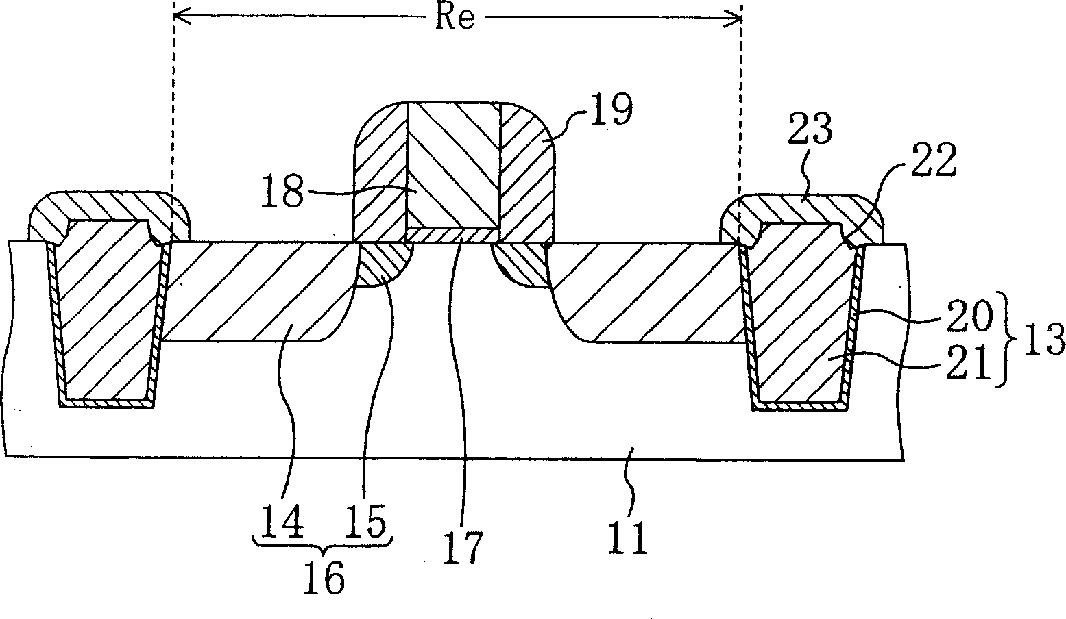
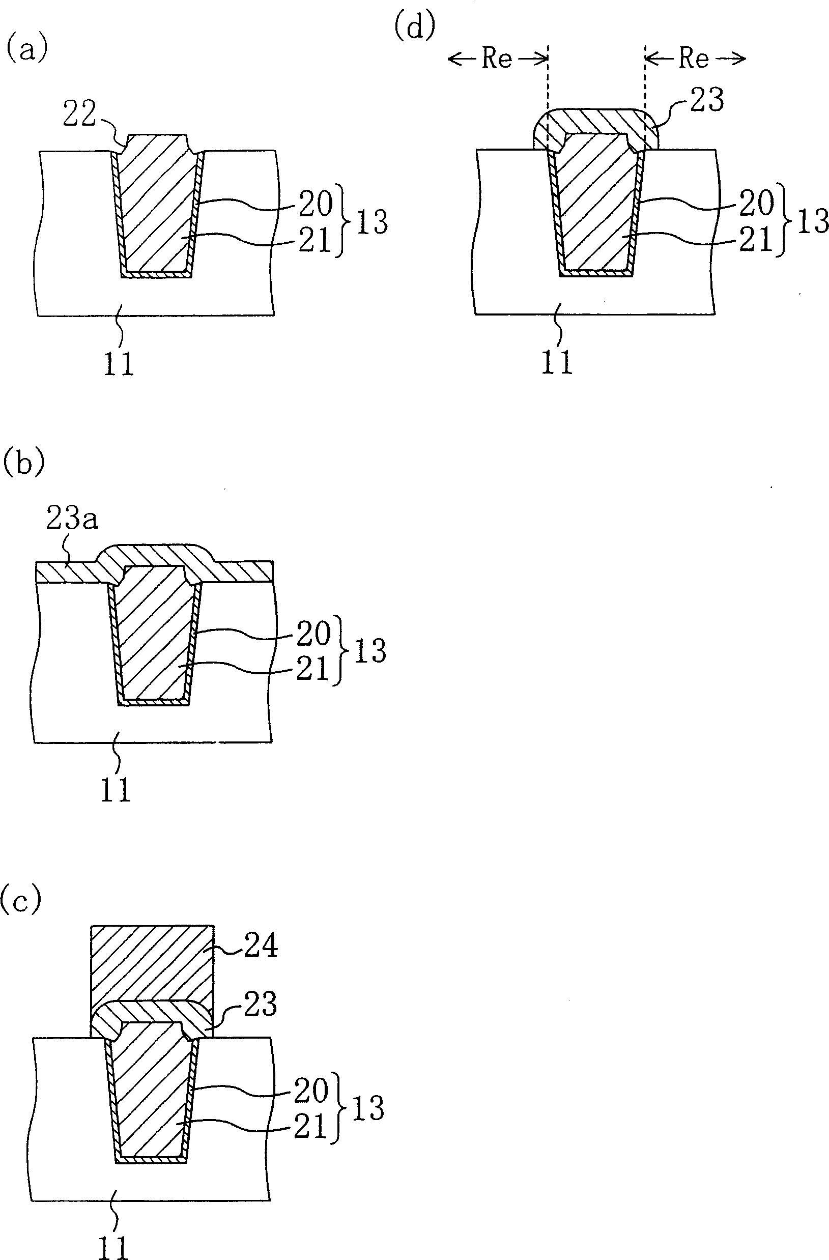
[0044] The semiconductor device of this embodiment is characterized in that the upper surface from the trench element isolation part to the surrounding area of ​​the trench element isolation part located in the element formation region is covered with an oxygen permeation inhibiting film that inhibits supply of oxygen. The following refers to the structure of the semiconductor device of this embodiment figure 1 Be explained. figure 1 It is a cross-sectional view showing the structure of the semiconductor device according to the first embodiment.

[0045] Such as figure 1 As shown, the semiconductor device of this embodiment is constituted by a MISFET provided in the element formation region Re of the semiconductor substrate 11 and a trench element isolation portion 13 surrounding the side surface of the element formation region Re.

[0046] The MISFET is an N-type source-drain region 16 composed of a high-concentration impurity diffusion layer 14 and a low-concentration i...

Embodiment 2

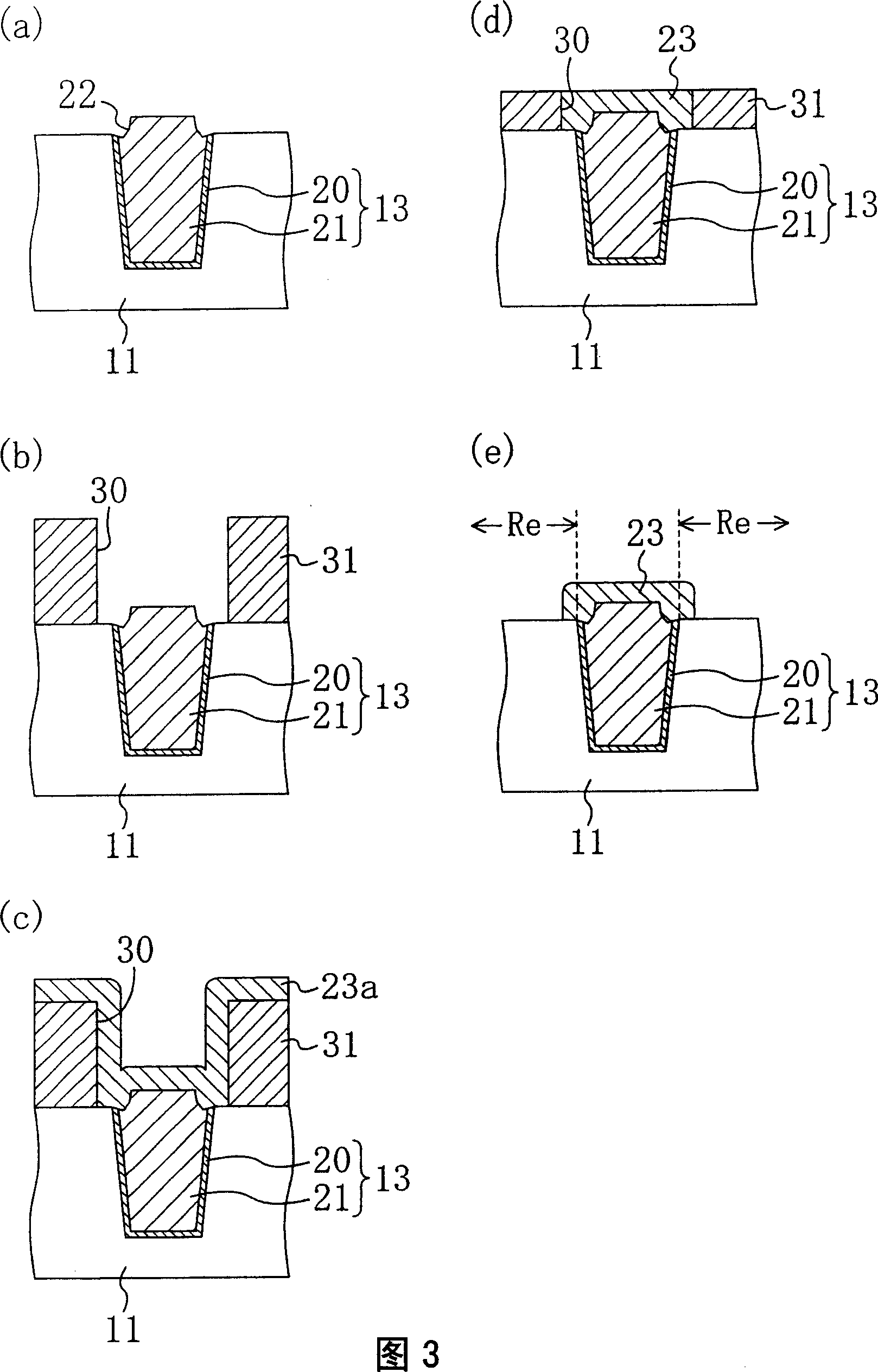
[0067] In this embodiment, a case where the oxygen gas permeation suppressing film is used to cover not the entire upper part of the trench device isolation part but only the boundary part between the trench device isolation part and the device isolation part forming region will be described.

[0068] Figure 4 It is a cross-sectional view showing the structure of the semiconductor device of the second embodiment.

[0069] Such as Figure 4 As shown, in the semiconductor device of this embodiment, the step portion 22 is formed on the outer edge portion of the trench device isolation portion 13 . Usually, the level difference portion 22 is naturally formed when the protective oxide film covering the element formation region Re of the semiconductor substrate 11 is removed during the formation process of the trench element isolation portion 13 . However, the step portion 22 may be gradually formed during other steps, or may be formed intentionally. The oxygen gas passage suppr...


PUM


Abstract

A semiconductor device of the present invention includes a MISFET provided in an element formation region Re of a semiconductor substrate 11 and a trench isolation 13 surrounding the sides of the element formation region Re. An oxygen-passage-suppression film 23 is provided from the top of the trench isolation 13 to the top of a portion of the element formation region Re adjacent to the trench isolation 13. The oxygen-passage-suppression film 23 is made of a silicon nitride film or the like through which oxygen is less likely to permeate. Therefore, since it becomes hard that the upper edge of the element formation region Re of the semiconductor substrate 11 is oxidized, an expansion of the volume of the upper edge is suppressed, thereby reducing a stress.

Description

technical field [0001] The present invention relates to a semiconductor device and its manufacturing method, and more particularly to a semiconductor device having a trench element isolation structure and its manufacturing method. Background technique [0002] As one of methods for electrically isolating elements on a semiconductor substrate, there is a trench element isolation method. The so-called trench device isolation method is a method of digging trenches of appropriate depth in the region between devices and embedding insulators therein to separate devices from each other (for example, refer to Patent Document 1). [0003] Next, a method of manufacturing a trench device isolation structure in a conventional semiconductor device will be described with reference to FIGS. 5( a )-( f ). 5( a )-( f ) are cross-sectional views showing the manufacturing process of the trench device isolation structure of the conventional semiconductor device. [0004] First, in the process...

Claims


Application Information

Patent Timeline
IPC IPC(8): H01L21/76H01L21/762H01L21/8234H01L29/78
CPCH01L21/76224H01L21/823481H01L29/78
Inventor 今出昌宏海本博之
Owner PANASONIC CORP
Learn More