Mounting device and structure for semiconductor component, electro-optical device and producing method thereof

An installation method and installation structure technology, which are applied in the fields of semiconductor/solid-state device manufacturing, semiconductor devices, and semiconductor/solid-state device components, etc., can solve problems such as poor short circuits, reduced reliability of conductive joints, and deterioration of product yields.

Inactive Publication Date: 2004-04-21
BOE TECH GRP CO LTD
View PDF0 Cites 3 Cited by
  • Summary
  • Abstract
  • Description
  • Claims
  • Application Information

AI Technical Summary

Problems solved by technology

[0006] In this situation, because it is difficult to sufficiently ensure the width, interval, etc. of the wiring terminals 121, 125 of the wiring board 120 and the electrodes 131, 135 of the semiconductor device 130, the conductive contact between the wiring terminals and the electrodes is poor, and adjacent Short-circuit defects between wiring terminals or electrodes increase, and there is a problem that the reliability of the conductive joint part of the semiconductor mounting structure is reduced, and the yield of the product is deteriorated.

Method used


Image

  • Mounting device and structure for semiconductor component, electro-optical device and producing method thereof
  • Mounting device and structure for semiconductor component, electro-optical device and producing method thereof
  • Mounting device and structure for semiconductor component, electro-optical device and producing method thereof

Examples


Embodiment Construction

[0066] Embodiments of a semiconductor device mounting method, a semiconductor device mounting structure, an electro-optical device, and an electronic device according to the present invention will be described in detail below with reference to the accompanying drawings.

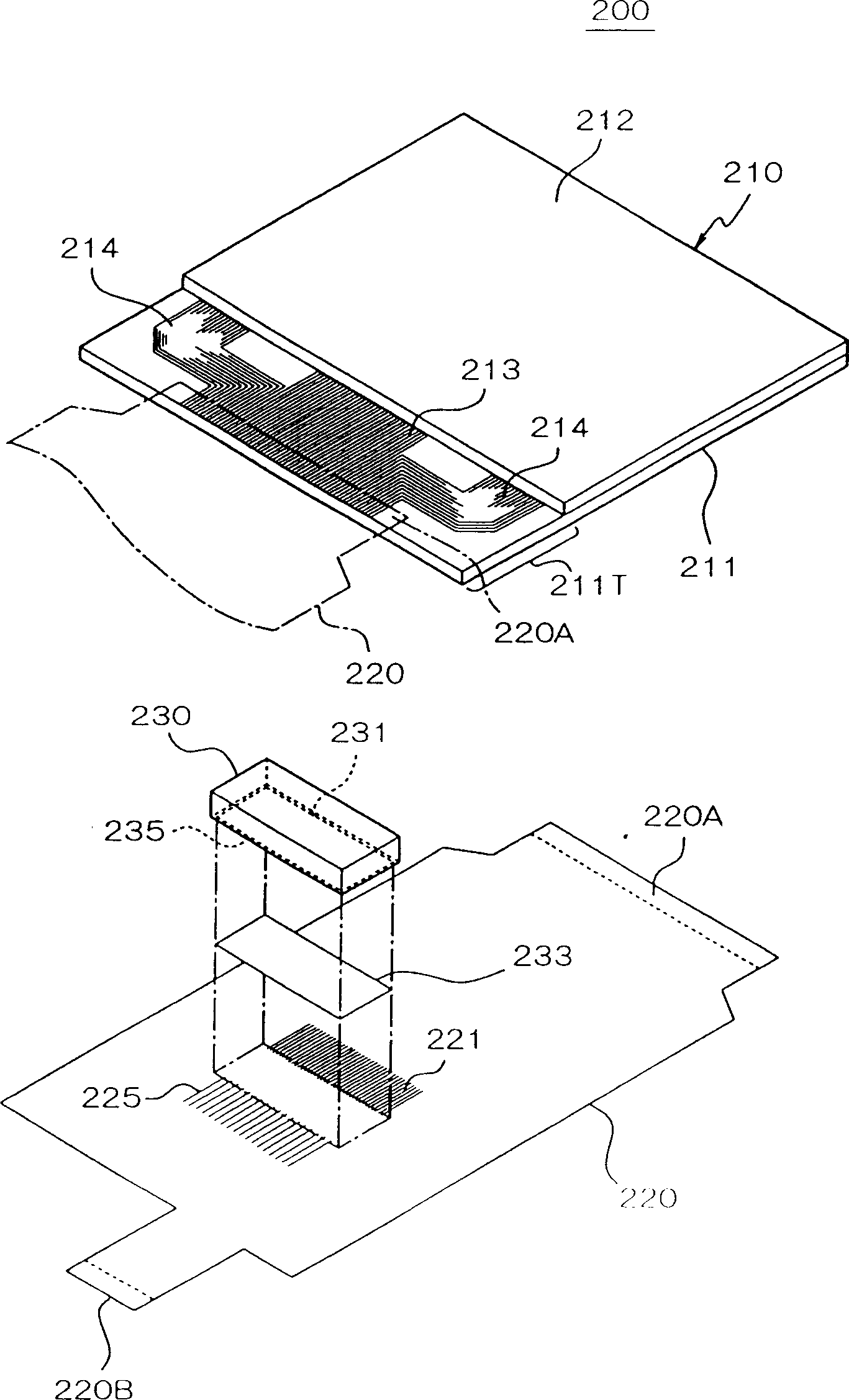
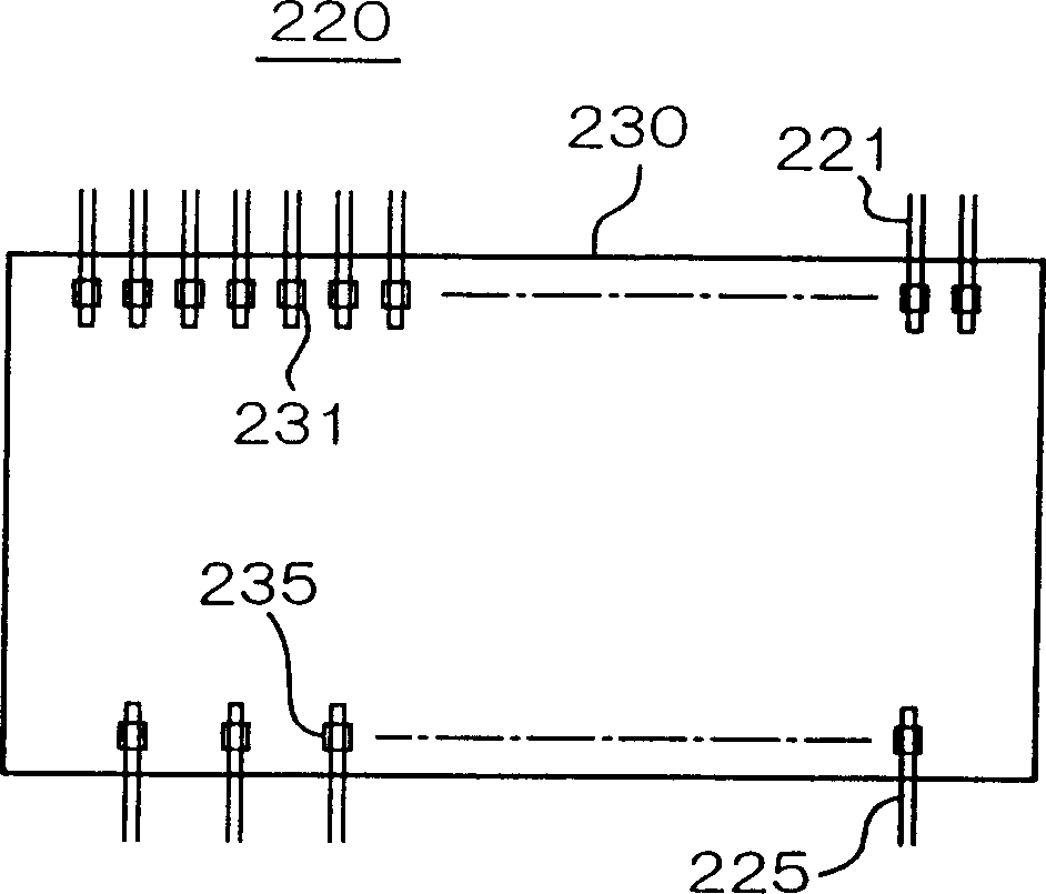
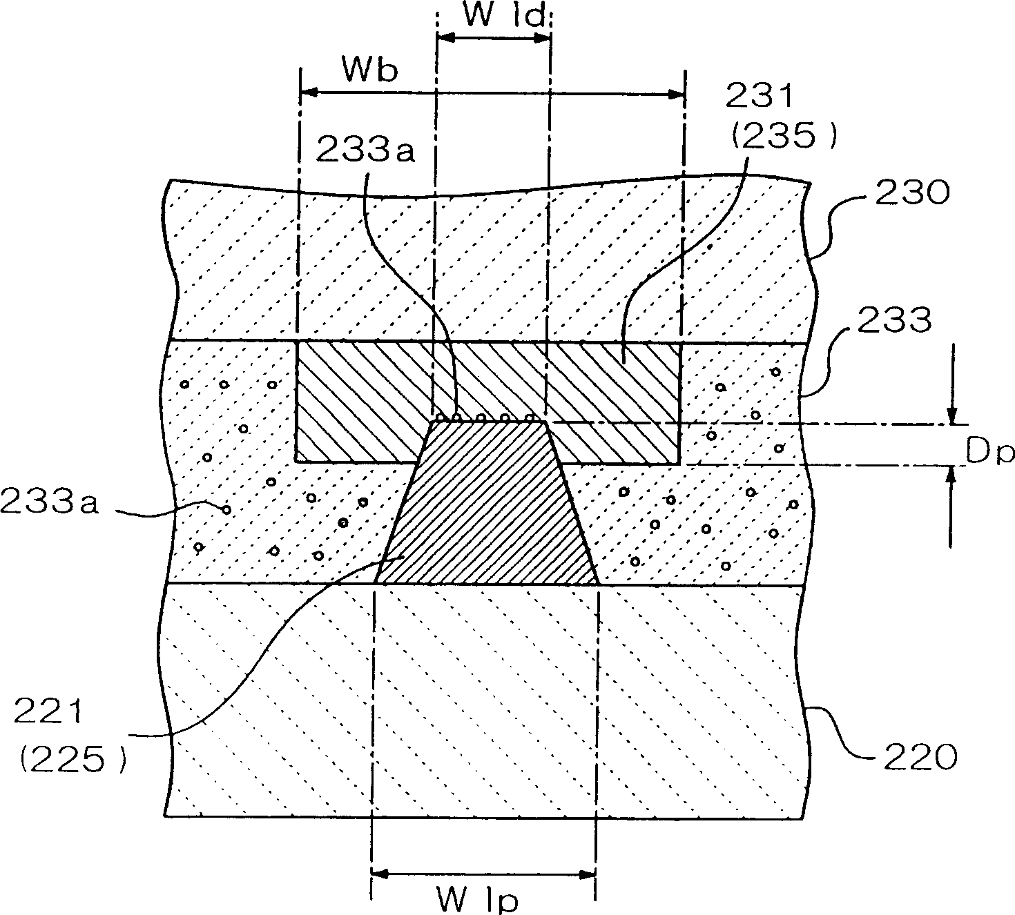
[0067] figure 1 It is an exploded perspective view showing the overall configuration of the liquid crystal device 200 as the electro-optical device of the present embodiment. This liquid crystal device 200 includes a liquid crystal panel 210 , a wiring board (wiring board) 220 connected to the liquid crystal panel 210 , and a semiconductor device (semiconductor bare chip) 230 mounted on the wiring board 220 .

[0068] In the liquid crystal panel 210 , substrates 211 and 212 made of transparent glass, plastic, or the like are bonded together with a sealing material (not shown), and liquid crystal (not shown) is sealed therein. In this liquid crystal panel 210, depending on the liquid crystal mode, a polarizi...


PUM

PropertyMeasurementUnit
heightaaaaaaaaaa

Abstract

The invention seeks to provide a new semiconductor device mounting method, a semiconductor device mounting structure, an electro-optical device and an electronic device that can improve the reliability of conductively joined portions, even if the numbers of wiring terminals and electrodes increases and intervals therebetween are narrowed. A wiring terminal is formed on a wiring substrate, and an electrode is formed on a semiconductor device. Here, the width of the wiring terminal is formed so that it becomes smaller than the width of the electrode. When the semiconductor device is mounted on the wiring substrate, the wiring terminal becomes embedded in the electrode due to applied pressure. It is preferable for the embedding amount of the wiring terminal to be within the range of about 1 µm to 5 µm.

Description

technical field [0001] The present invention relates to a method for mounting a semiconductor device, a mounting structure for a semiconductor device, an electro-optic device and electronic equipment, and a method for manufacturing an electro-optic device, in particular to a method for directly mounting a semiconductor device on a substrate and a mounting structure for the semiconductor device on the substrate. Background technique [0002] In general, there is a method of directly mounting a semiconductor device on a substrate, such as a flip chip mounting method. In this mounting method, while electrodes are provided on a semiconductor device (bare chip), wiring (wiring) terminals are formed on a substrate, and electrodes and wiring terminals are directly conductively contacted without via leads (ヮィャ). In this method, on a semiconductor device, an electrode having a protruding shape called a bump electrode is often formed, and the protruding electrode is directly contacted...

Claims


Application Information

Patent Timeline
Patent Type & Authority Applications(China)
IPC IPC(8): G02F1/1345G02F1/13G02F1/1362G09F9/00H01L21/60H01L21/603H01L23/00H01L23/485H01L23/498H05K3/32
CPCH01L2924/01015H01L2224/83851H01L24/28H01L2924/0105H01L2924/01082H01L2224/81193H01L2924/0781H01L2924/01004H01L2224/13012H01L2924/12041H01L2224/16H01L2224/81903G02F1/13452H01L2224/13144H01L2924/01029H01L2224/29111H01L2224/29355H01L2224/13099H01L2924/0132H01L23/562H05K2201/10674H05K3/325H01L2224/13016H01L2924/014H01L2924/01013H05K2201/09427H01L2224/2929H01L2924/01047H01L2924/01079H01L24/13H01L23/498H01L24/16H01L2224/838H01L24/83H01L2924/1579H01L2924/01005H01L2924/01033H01L2924/01006H01L2924/01078H01L2224/8319H01L2924/12044H01L2224/13076H01L2224/13078H01L2224/05573H01L2224/05568H01L2924/00014H01L2224/16105H01L2224/81194H01L2224/05556H01L24/05H01L2224/05599
Inventor 山田一幸芦田刚士中泽政彦汤本正则
Owner BOE TECH GRP CO LTD
Why Eureka
Try Eureka