
AC drive type plasma display device for electro-optical plate and its manufacturing method

An AC drive and plasma technology, applied in the direction of AC plasma display panel, plasma, electrode system manufacturing, etc., can solve the problem of driving voltage increase

Inactive Publication Date: 2003-07-16
SCI ADVENTURE TECH C KR
View PDF0 Cites 1 Cited by
  • Summary
  • Abstract
  • Description
  • Claims
  • Application Information

AI Technical Summary

Problems solved by technology

[0011] However, as the discharge cell (cell) becomes millimeter (mm) in size, the height of the discharge cell (cell) also needs to be increased accordingly, resulting in the need to apply a high voltage of nearly 1kV between the two electrodes in order to excite the gas discharge; However, capacitive devices with a layered structure of front glass substrate / display electrode (transparent electrode) / transparent dielectric / discharge tank (cell) / phosphor / white dielectric / address electrode (metal electrode) / back glass substrate In the PDP display device, the voltage applied to the discharge cell (cell) varies when the thickness of the dielectric layer is thinner, and the height of the discharge cell (cell) with a thicker dielectric layer is larger than the thickness of the dielectric layer. It becomes larger; recently, only the front glass substrate structure of the PDP display device is changed, and a glass substrate is manufactured, that is, the front glass substrate structure of the PDP display device is constructed to display electrodes (transparent electrodes) / front glass substrate / discharge tank (cell) / phosphor / white dielectric / address electrode / back glass substrate, although it is also suitable for PDP electro-optical panels, but once it is used as a transparent dielectric, the front glass substrate (several millimeters (mm) thick) is relatively thick When thick and the discharge groove (cell) is small, the driving voltage indicated above will increase significantly

Method used


Image

  • AC drive type plasma display device for electro-optical plate and its manufacturing method
  • AC drive type plasma display device for electro-optical plate and its manufacturing method
  • AC drive type plasma display device for electro-optical plate and its manufacturing method

Examples


Embodiment Construction

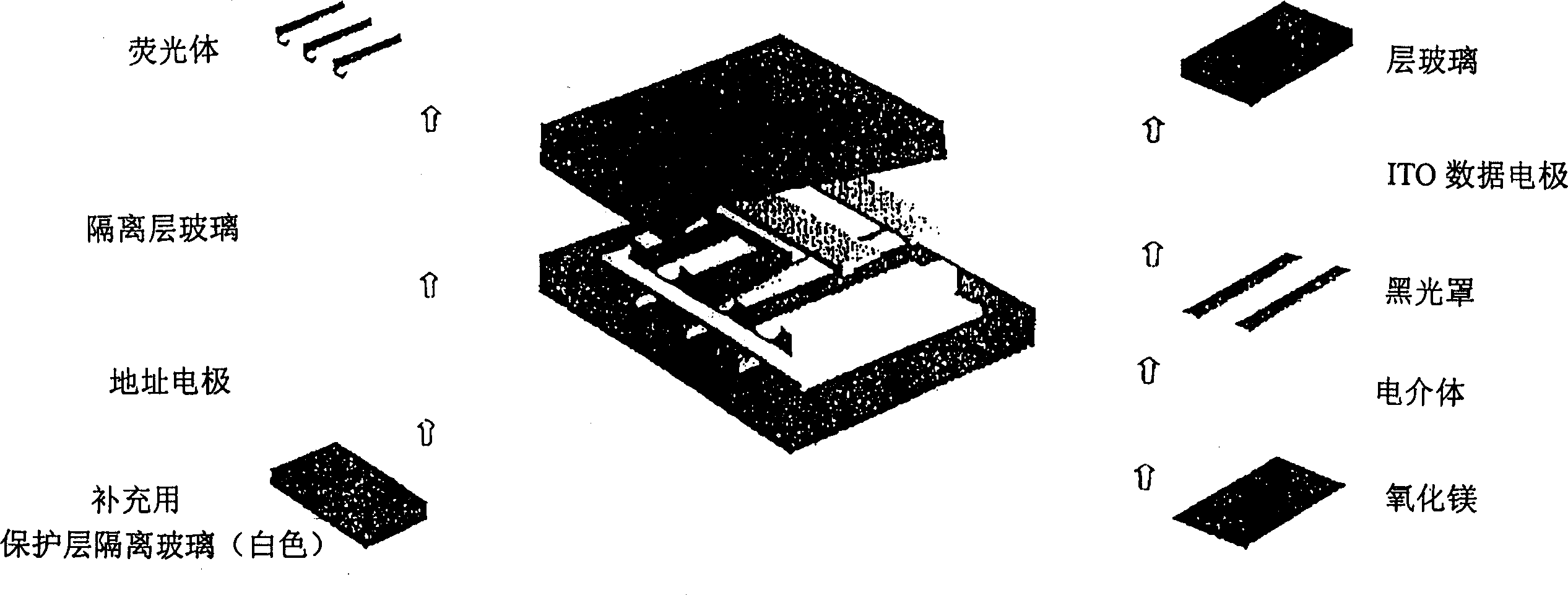
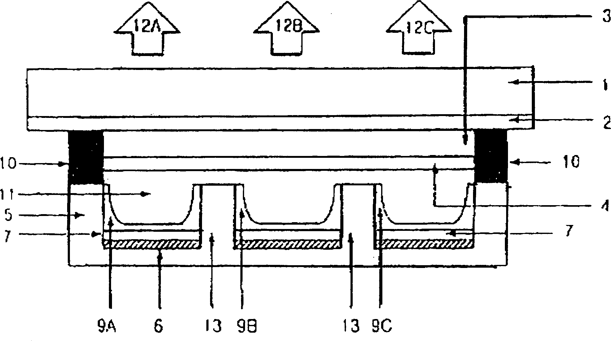
[0028] figure 2 It is an exploded perspective view of an AC-driven plasma display device for an electro-optical panel of the present invention, image 3 for the sectional view.

[0029] figure 2 It is the structure of the known PDP display device for wall-mounted TVs, which is improved to be suitable for PDP electro-optic panels, that is, a PDP electro-optic panel structure that can be driven at low voltage and can be manufactured at low cost; it basically has a front glass substrate / transparent Structure of electrode / transparent dielectric / protective film / discharge tank (cell) / phosphor / white dielectric / metal electrode / back glass substrate (the front glass substrate 1 shown in the figure can actually be rotated by 90 degrees) .

[0030] Therefore, the structural feature of the present invention is that the front glass substrate 1 after cutting is formed with a transparent electrode 2 and a protective film 4 above and below it; and the back glass substrate 5 that is also c...


PUM


Abstract

An AC driven plasma display device for electroluminescent board features that its external surface has transparent electrode and metal electrode, the back of the glass plate parallel to said electrodes is machined to form slots, which are joined to form discharge cell, and the upper and lower substrates instead of partition, transparent dielectric and white dielectric constitute a dielectric bandlayer which is machined to form discharge cell to expose the electrodes to the outside of discharge cell. Its advantages are simple making method, low cost and low drive voltage. It is suitable for outdoor signboard, railway timetable, etc.

Description

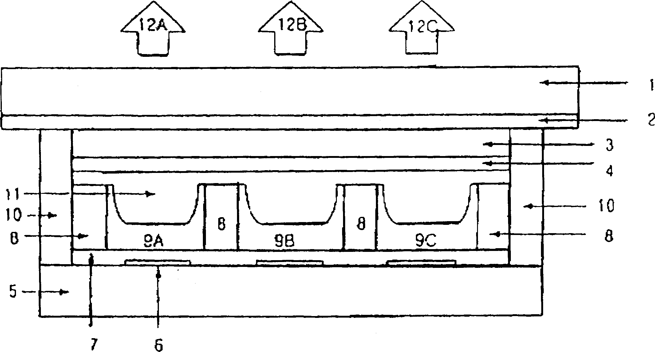
technical field [0001] The present invention relates to an AC-driven plasma display device (Plasma Display Panel, PDP) for an electro-optical panel and a manufacturing method thereof. An AC-driven plasma display device for an electro-optic panel of a public billboard such as a billboard and a manufacturing method thereof. Background technique [0002] Such as figure 1 In the cross-sectional view of the known AC-driven plasma device (hereinafter referred to as "PDP display device") used in wall-mounted TVs or PC displays, it is composed of an upper plate and a lower plate, wherein the upper plate is made of: a glass substrate on the front 1, a transparent display electrode 2 formed by vacuum evaporation; and a glassy transparent dielectric layer 3 formed by thick film firing by screen printing and other methods in order to limit the inflow of current during AC driving; and a gas During discharge, in order to protect the transparent dielectric layer 3, it is composed of a pr...

Claims


Application Information

Patent Timeline
IPC IPC(8): H05H1/46H01J9/02H01J9/24H01J11/12H01J11/22H01J11/24H01J11/26H01J11/34H01J11/36H01J11/38H01J11/40
CPCH01J9/241H01J11/34H01J11/12
Inventor 李俊世
Owner SCI ADVENTURE TECH C KR
Learn More