Drive technique for starting liquid crystal device
A liquid crystal device and liquid crystal layer technology, applied in nonlinear optics, instruments, optics, etc., can solve the problems that liquid crystal has not yet reached the level of general use, the technology has not been realized, and the price has increased.
- Summary
- Abstract
- Description
- Claims
- Application Information
AI Technical Summary
Problems solved by technology
Method used
Image

Examples
Embodiment 1-1
[0078] Here, "(Example 1-1)" means "Example 1 of the first invention group". Therefore, if it is 'Example 2 of Invention Group 1', it will be described as '(Example 1-2)'. The same is true for other invention groups.
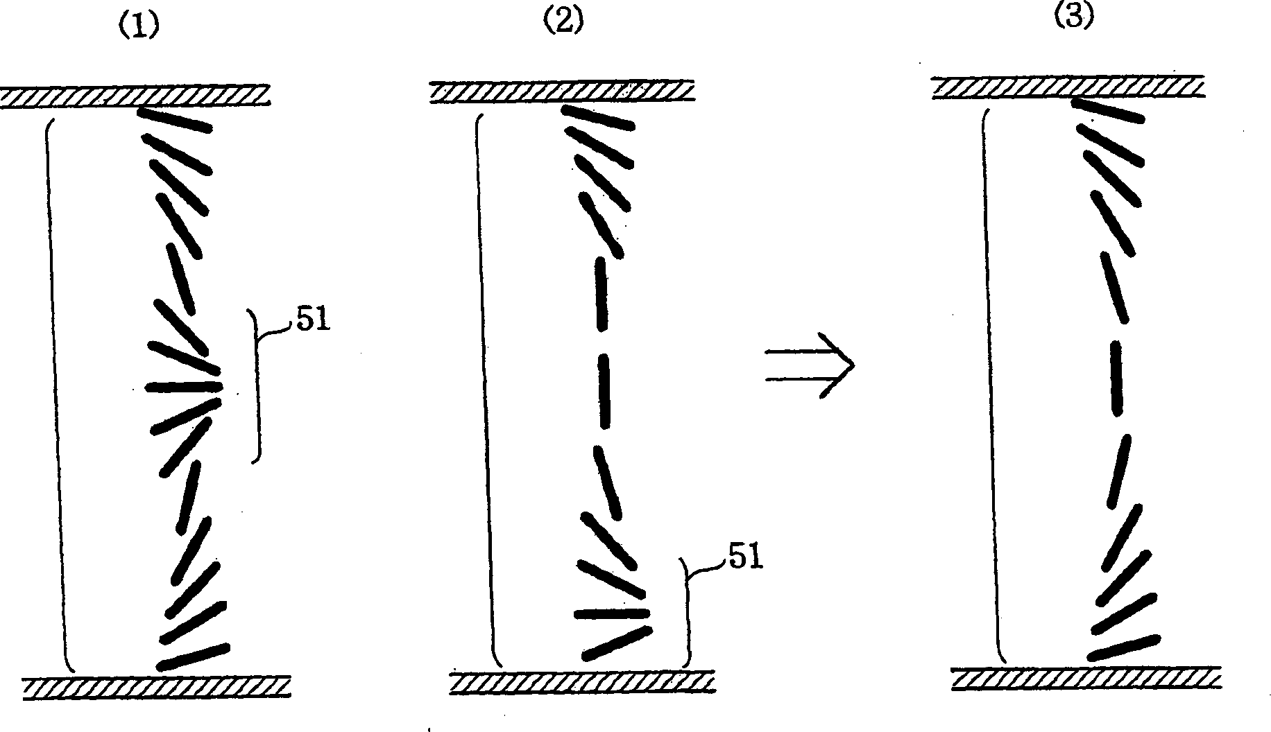
[0079] In addition, in fact, although the pixels composed of such a circuit are formed in several columns and rows vertically and horizontally on the substrate, and in some cases, many levels are formed, but since it is self-explanatory and it is troublesome to draw them all, the figure is omitted. This procedure is also the same in other groups of inventions or other embodiments.
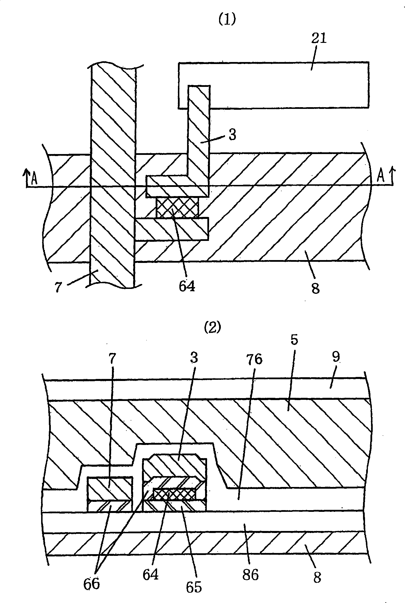
[0080] figure 2 A plane (1) showing the structure of one pixel of a conventional liquid crystal panel and an A-A section (2) of a transistor device portion are shown. In this figure, 21 is a transparent pixel electrode. 3 is a pixel electrode. 5 is a liquid crystal layer. 64 is a channel protection film. 65 is an a-Si (amorphous silicon) layer. 66 is an n+a-Si layer. 7 is ...
Embodiment 1-2
[0100] Figure 5 The configuration of Embodiment 1-2 of the present invention is shown.
[0101] In this figure, 8 is the gate line electrode, 7 is the source line electrode, 3 is the pixel electrode, 64 is the channel protective film, 65 is the a-Si layer, 66 is the n+a-Si layer, 86 is the The insulating film between the gate line electrode and the a-Si layer, 76 is the insulating film between the source line electrode and the liquid crystal layer, 5 is the liquid crystal layer, 9 is the opposite electrode, 21 is the transparent pixel electrode, and A is a cross section part of the line.
[0102] In the previous embodiment 1 (Since there is no misunderstanding, the embodiment 1-1 is abbreviated as this. The following is also the same.), although the insulating film is made into two layers, but, by means of this Figure 5 The same effect can be obtained by reducing the thickness of the insulating film between the gate electrode and the liquid crystal layer by patterning as s...
Embodiment 1-3
[0104] Figure 6 The configurations of Embodiments 1-3 of the present invention are shown.
[0105] In this figure, also with Figure 5 Same, 8 is gate line electrode, 7 is source line electrode, 3 is pixel electrode, 64 is channel protection film, 65 is a-Si layer, 66 is n+a-Si layer, 86 is gate line The insulating film between the electrode and the a-Si layer, 76 is the insulating film between the source line electrode and the liquid crystal layer, 5 is the liquid crystal layer, 9 is the opposite electrode, 21 is the transparent pixel electrode, and A is a line showing a section.
[0106] In the case of this structure, the thickness of the liquid crystal layer above the gate line can be made thinner by making the gate line of a predetermined partial thick-film type thicker than the film thickness of the gate line electrode, which can increase the thickness of the gate line. The intensity of the electric field applied to the liquid crystal layer enables rapid transition to ...
PUM
| Property | Measurement | Unit |
|---|---|---|
| relative permittivity | aaaaa | aaaaa |
Abstract
Description
Claims
Application Information
 - Generate Ideas
- Intellectual Property
- Life Sciences
- Materials
- Tech Scout
- Unparalleled Data Quality
- Higher Quality Content
- 60% Fewer Hallucinations
Browse by: Latest US Patents, China's latest patents, Technical Efficacy Thesaurus, Application Domain, Technology Topic, Popular Technical Reports.
© 2025 PatSnap. All rights reserved.Legal|Privacy policy|Modern Slavery Act Transparency Statement|Sitemap|About US| Contact US: help@patsnap.com