Over-voltage protector circuit with output buffer

A technology of protection circuit and output buffer, which is applied in the fields of logic circuit coupling/interface, logic circuit connection/interface arrangement, pulse technology, etc. using field effect transistors to prevent leakage current, save use area, and avoid component damage.

Inactive Publication Date: 2006-06-28
VIA TECH INC
View PDF0 Cites 0 Cited by
  • Summary
  • Abstract
  • Description
  • Claims
  • Application Information

AI Technical Summary

Problems solved by technology

[0009] The present invention is to provide an output buffer overvoltage protection circuit to solve the technical problem that the core circuit of the chip will not be damaged due to excessive external working voltage

Method used


Image

  • Over-voltage protector circuit with output buffer
  • Over-voltage protector circuit with output buffer
  • Over-voltage protector circuit with output buffer

Examples


Embodiment Construction

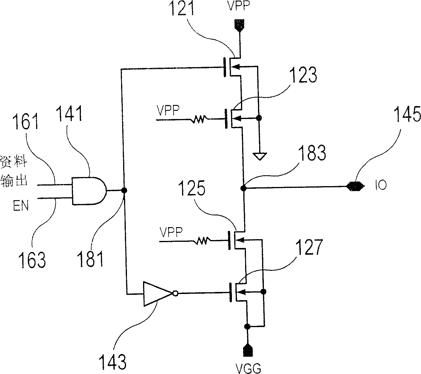
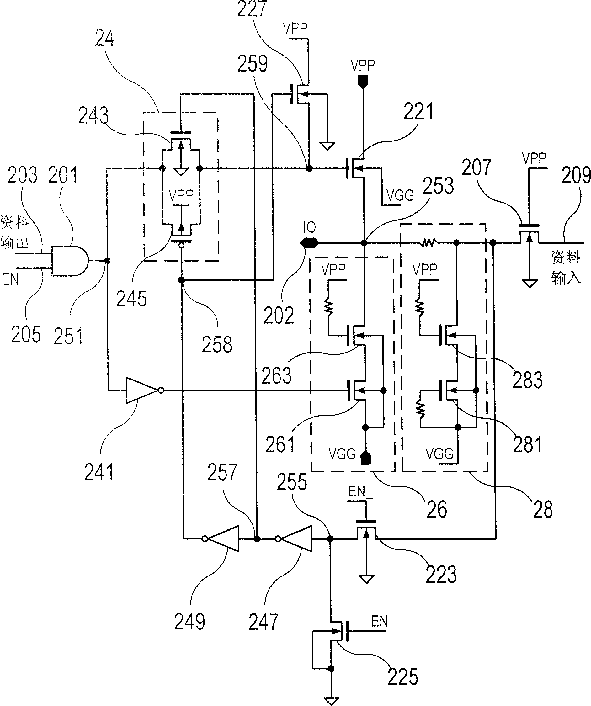
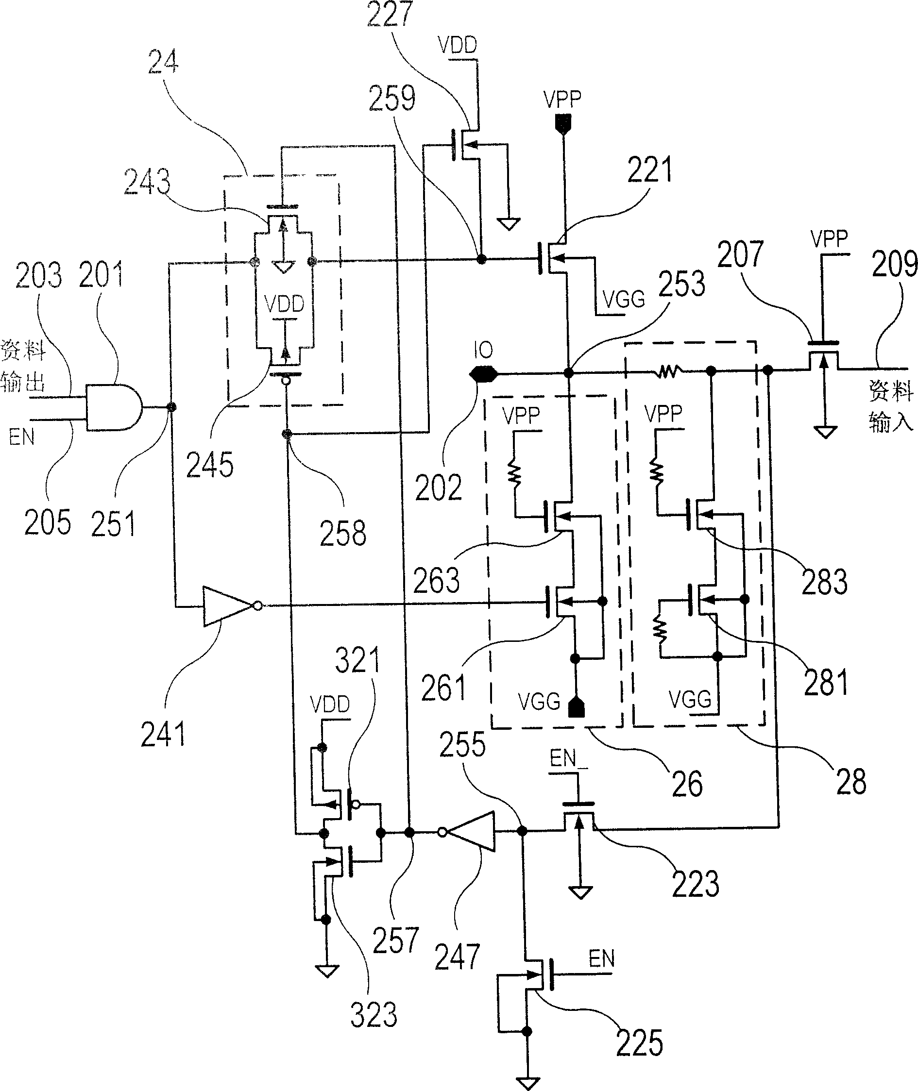
[0035] First, see figure 2 Shown is a circuit diagram of a preferred embodiment of the present invention. As shown in the figure, its data output element includes an AND gate 201, its two input ends are respectively connected to a data output line 203 and an output control line 205, and its output end is connected to a node 251, and then respectively connected to a pull-up circuit and an output control line 205. The pull-down circuit can control whether the data is output or not by the control signal EN (output enable) of the output control line 205 and the function of the AND gate. The I / O pin 202 is connected to an I / O node 253, and a pull-up transistor 221 is connected between the I / O node 253 and the external working potential VPP. The drain of the pull-up transistor 221 is connected to the external working potential VPP, the source is connected to the I / O node 253 , and the gate receives the output signal of the data output element through a boost node 259 . The pull-u...


PUM


Abstract

The over-voltage protection circuit with its output buffered is positioned between the element for outputting data and the output / input node, which is connected to the output / input pin. The circuit includes a pull up transistor, a boost transistor and a boost control circuit. The drain electrode of the pull up transistor is connected to an external operating potential, the source electrode is connected to the output / input node and the grid electrode is connected to the element for outputting data through the voltage-boosting node. The drain electrode for the boost transistor is connected to an external operating potential, and the source electrode is connected to the voltage-boosting node. The input end of the boost control circuit is connected to the output / input node, and the output end is connected to the grid electrode of the boost transistor.

Description

technical field [0001] The invention relates to a protection circuit, in particular to an output buffer overvoltage protection circuit. Background technique [0002] In recent years, due to the rapid development of electronics and information-related industries and the trend of various products becoming thinner and smaller, people tend to integrate more and more electronic components into one chip, resulting in a significant increase in the density of components in the chip. At the same time, information products The computing speed is also continuously improved with the needs of people. In order to cope with the high density of components in the chip and the high-speed calculation rate, it is necessary to use a voltage lower than the known specifications in the chip to work, which often causes a difference between the internal operating voltage of the chip and the external operating voltage, so it must be used in the chip. A buffer circuit is provided at the junction of th...

Claims


Application Information

Patent Timeline
Patent Type & Authority Patents(China)
IPC IPC(8): H03K19/0175H03K17/08H03K19/0185
Inventor 林明德颜敬贤
Owner VIA TECH INC
Why Eureka
Try Eureka