
Manufacturing method of semiconductor laser device

A technology of laser devices and manufacturing methods, which is applied in the direction of semiconductor laser devices, semiconductor lasers, and structural details of semiconductor lasers, and can solve problems such as reducing printing quality

Inactive Publication Date: 2006-06-21
SHARP KK
View PDF4 Cites 0 Cited by
  • Summary
  • Abstract
  • Description
  • Claims
  • Application Information

AI Technical Summary

Problems solved by technology

This reduces the print quality

Method used


Image

  • Manufacturing method of semiconductor laser device
  • Manufacturing method of semiconductor laser device
  • Manufacturing method of semiconductor laser device

Examples


Embodiment Construction

[0059] One embodiment of the present invention will be described below.

[0060] The semiconductor laser device (this laser device) according to this embodiment is a multi-beam laser device capable of simultaneously emitting two laser beams.

[0061] Moreover, this device can be used in electronic equipment such as a player capable of reproducing both CD (compact disc) and DVD (digital versatile disc), and a laser beam printer (digital copier, etc.) that exposes a photoreceptor by two types of laser light.

[0062] First, the configuration of this laser device will be described.

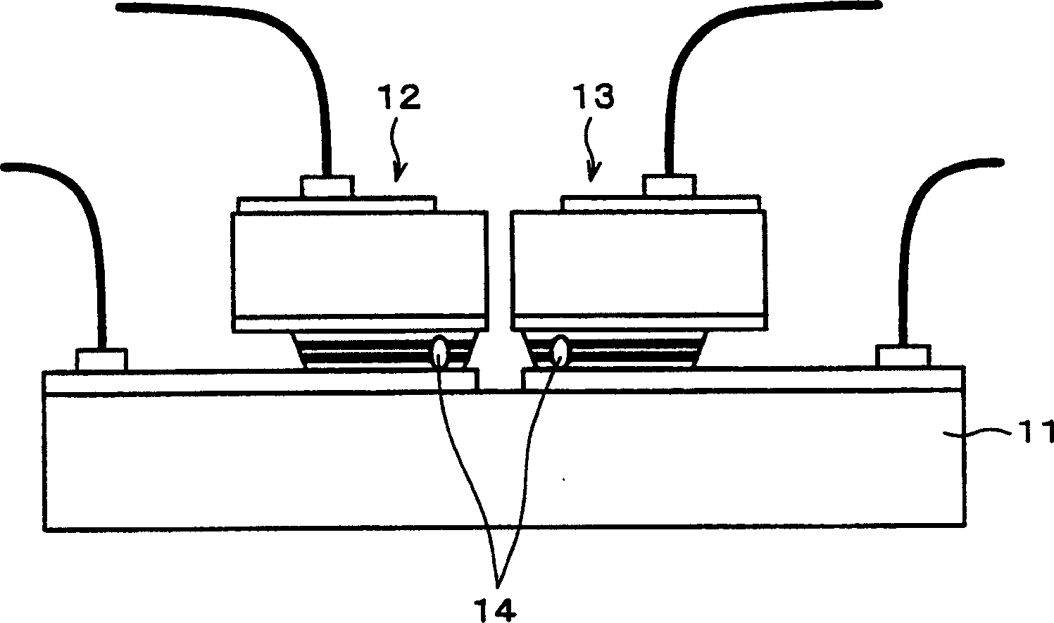
[0063] figure 1 It is an explanatory diagram of the structure of this laser device.

[0064] As shown in the figure, the first semiconductor laser element 12 and the second semiconductor laser element 13 are mounted on a submount (submount substrate) 11 formed of insulating SiC.

[0065] In addition, the present laser device outputs laser light from respective light-emitting points (oscillating r...


PUM

PropertyMeasurementUnit
diameteraaaaaaaaaa
luminous pointaaaaaaaaaa

Abstract

The present invention provides a method of manufacturing a semiconductor laser device. First, a light emitting portion is formed on a single substrate and mounted on a sub-mount. Then, the substrate mounted on the sub-stage is cut from an intermediate position between the light emitting parts. In the laser device manufactured in this way, since the two laser elements are formed on a single chip, the relative positional accuracy between them can be improved. Since the substrate is cut between the laser elements, heat conduction and electrical crosstalk through the substrate can be significantly suppressed, so the relative positional accuracy of multiple laser elements can be ensured to a high degree, and the influence of crosstalk can be suppressed.

Description

technical field [0001] The present invention relates to a method of manufacturing a semiconductor laser device including a plurality of semiconductor laser elements on a sub-mount. Background technique [0002] In the past, for example, as shown in Document 1 (Japanese Laid-Open Patent Gazette; Japanese Unexamined Patent Publication No. 3-145779, publication date; June 20, 1991), a laser device (multi-beam laser device; MB laser device). [0003] Such MB laser devices are used, for example, in players capable of reproducing both CDs and DVDs, and laser beam printers (LBP; digital copiers, etc.) that expose photoreceptors with two laser beams. [0004] In addition, when such an MB laser device is used in the above-mentioned player, the two types of laser beams have different wavelengths. [0005] Also, when used on a printer, 2 laser beams will be emitted simultaneously. Therefore, it is necessary to have a configuration capable of driving the two laser elements independen...

Claims


Application Information

Patent Timeline
Patent Type & Authority Patents(China)
IPC IPC(8): H01S5/022H01S5/00G11B7/125G11B7/1275H01S3/04H01S5/02H01S5/40
CPCG11B7/1275H01S5/0201H01S5/02212H01S5/06832H01S5/2231H01S5/4031H01S5/4087H01L2224/32145H01L2224/48091H01L2224/45144H01S5/0234H01S5/02325H01S5/0237H01L2924/00014H01L2924/00
Inventor 冈崎淳
Owner SHARP KK
Learn More