
Non-volatile memory with float gate wall and its preparing process

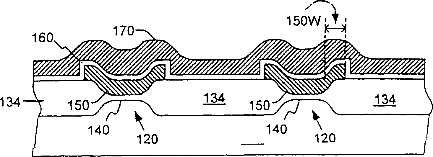
A non-volatile, manufacturing method technology, used in semiconductor/solid-state device manufacturing, electrical solid-state devices, semiconductor devices, etc.

Inactive Publication Date: 2006-04-12
PROMOS TECH INC
View PDF2 Cites 0 Cited by
  • Summary
  • Abstract
  • Description
  • Claims
  • Application Information

AI Technical Summary

Problems solved by technology

[0003] The field oxide layer 134 is formed by known LOCOS fabrication, and the field oxide region 134 and the active region 120 are formed using a different photomask from the later-formed floating gate 150 because of the misalignment of the photomask Therefore, the floating gate 150 is partially overlapped with the field oxide region 134. Although the overlapping portion ("wings") 150W of the floating gate 150 increases the size of the memory, it improves the performance of the floating gate 150 and the Capacitive coupling between control gates 170

Method used


Image

  • Non-volatile memory with float gate wall and its preparing process
  • Non-volatile memory with float gate wall and its preparing process
  • Non-volatile memory with float gate wall and its preparing process

Examples


Embodiment Construction

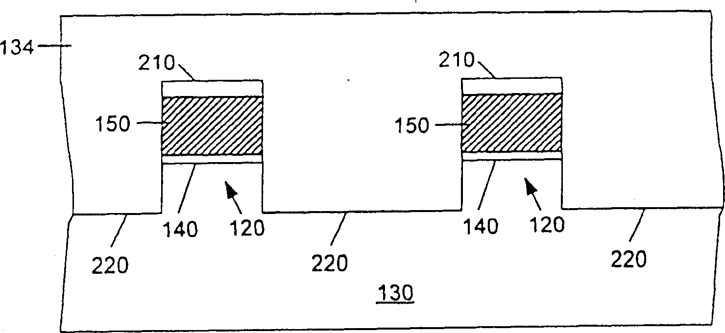
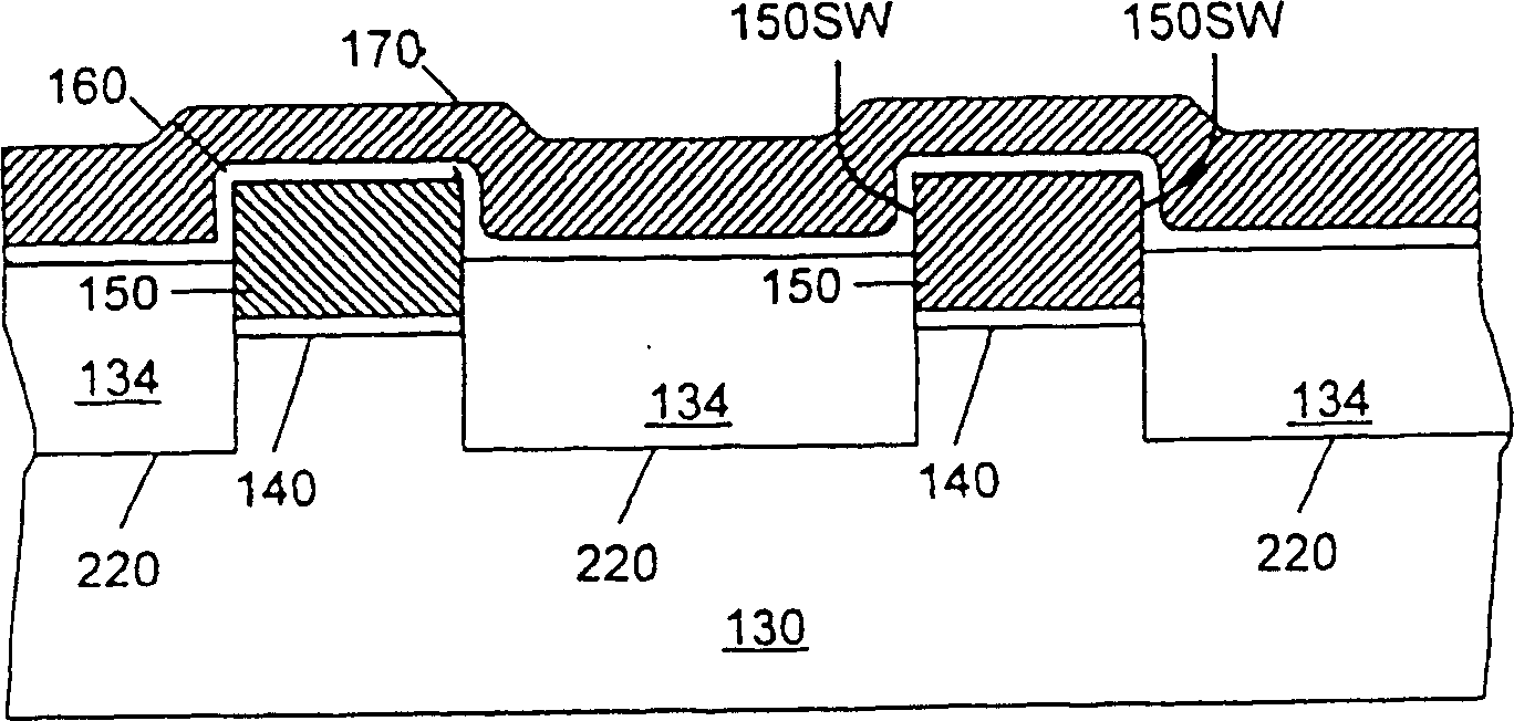
[0015] Figure 4 It is a cross-sectional view of a non-volatile memory structure generated in the pre-manufacturing stage. A floating gate polysilicon layer 150 self-aligned with the active region 120 is formed by known shallow trench isolation (shallow trench isolation, STI) technology, basically the same as figure 2 Similarly, in this embodiment, the substrate 130 is a suitably doped (such as doped with phosphorus) single crystal silicon substrate, and a suitable well (well) (not shown) can be formed in the substrate 130, as H.T.Tuan et al. Patent application No. 09 / 640,139 titled "Nonvolatile Memory Structures and Methods of Fabrication" (application date August 15, 2000) described in the patent, of course other types of substrates can also be used here, such as non-silicon substrates, the present The invention is not limited to a particular kind of well or doping pattern.

[0016] An insulating layer 140 is formed on the substrate 130. In this embodiment, the insulating ...


PUM


Abstract

A method for preparing a non-volatile memory with float grid and spacing wall includes such steps as generating the first material layer for providing part of float grid, generating L1 layer with exposed side wall, and generating a spacing wall on said side wall for providing the another part of float grid. Said non-volatile memoryc contains a float grid, an insulating layer surrounding the sides of float grid, and a control grid on the float grid.

Description

(1) Technical field [0001] The invention relates to a semiconductor technology, in particular to a non-volatile semiconductor memory. (2) Background technology [0002] figure 1 It is a cross-sectional view of a traditional non-volatile semiconductor memory. The field oxide region 134 is used to isolate the active area 120 and other active areas in the silicon substrate 130, and a gate is formed on the active area 120. oxide layer (gate oxide) 140, and then deposit a polysilicon layer 150 on the gate oxide layer 140, after patterning, a floating gate (floating gate) will be formed on each active region 120, and then in An insulating layer 160 is formed on the floating gate (such as an ONO layer, which is composed of a silicon dioxide layer, a silicon nitride layer and another silicon dioxide layer), and then a polysilicon layer 170 is deposited. Turn it into a control gate (control gate), please refer to the paper "A 0.67um2Self-Aligned Shallow Trench Isolation Cell (SA -...

Claims


Application Information

Patent Timeline
Patent Type & Authority Patents(China)
IPC IPC(8): H01L21/8239H10B99/00H01L21/28H01L21/8247H01L29/423H10B69/00
CPCH01L27/11521H01L21/28273H01L27/115H01L29/42324H01L29/42328H01L29/42336H01L29/40114H10B69/00H10B41/30
Inventor 段行迪詹费汉梁仲伟萧家顺
Owner PROMOS TECH INC
Learn More