
Method of improving reliability of flash memory

A memory and reliability technology, applied in the fields of semiconductor/solid-state device manufacturing, electrical components, circuits, etc., can solve the problems of excessive polishing of semiconductor wafers 10, high cost, decrease in good rate, etc., to improve random bit faults and improve product reliability. , the effect of simplifying the process

Inactive Publication Date: 2006-01-18
MACRONIX INT CO LTD
View PDF0 Cites 1 Cited by
  • Summary
  • Abstract
  • Description
  • Claims
  • Application Information

AI Technical Summary

Problems solved by technology

However, the CMP process may still cause over-polishing of some areas on the surface of the semiconductor wafer 10, resulting in a decrease in good rate and high cost.

Method used


Image

  • Method of improving reliability of flash memory
  • Method of improving reliability of flash memory
  • Method of improving reliability of flash memory

Examples


Embodiment Construction

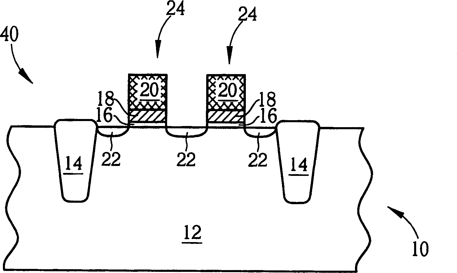
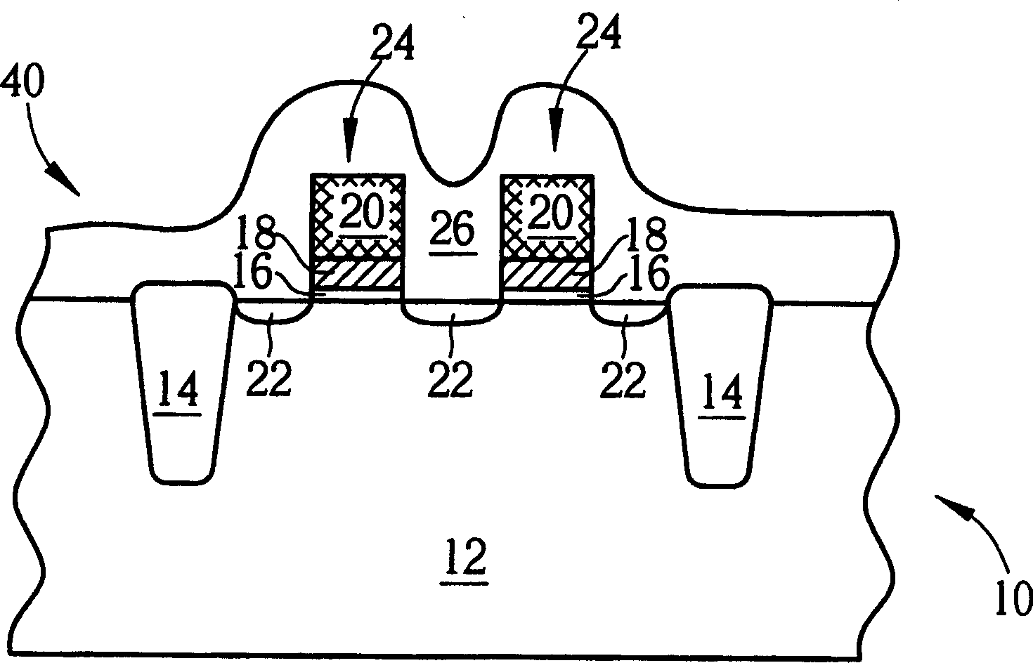
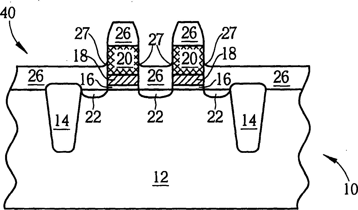
[0033] Please refer to Figure 8 to Figure 12 , Figure 8 to Figure 12 It is a schematic cross-sectional view of fabricating a high-reliability flash memory cell in a preferred embodiment of the method of the present invention. For the convenience of explaining the present invention, Figure 8 to Figure 12 Only a portion of the flash memory area relevant to the method of the present invention is shown. In the preferred embodiment of the method of the present invention, a dual-bit flash memory cell 110 is used as an example for illustration. First, as Figure 8 As shown, the semiconductor wafer 80 includes a silicon substrate 82, an active area on the silicon substrate 82 isolated by a shallow trench isolation (STI) region 84, and two gates Structure 94 is provided within the active area. The gate structure 94 has a gate oxide layer or tunnel oxide layer 86 disposed on the surface of the silicon substrate 82, a polysilicon layer or PL1 layer 88 disposed directly above the tu...


PUM


Abstract

The method of improving the reliability of flash memory includes the following steps: forming one stacked layer on one substrate including one first polysilicon layer and one sacrificial layer on the polysilicon layer, forming high temperature oxide (HTO) film to cover the stacked layer, depositing one dielectric layer on the HTO film, wet etching the dielectric layer and the HTO film to expose the sacrificial layer, eliminating the sacrificial layer completely and at least one pickling, soaking and cleaning process. The HTO film can strengthen the interface between the dielectric layer and the first polysilicon layer to avoid acid erosion cracking during the pickling, soaking and cleaning process.

Description

technical field [0001] The present invention provides a manufacturing method for improving the reliability of flash memory, and more particularly, to a method of utilizing an HTO (High Temperature Oxide) film to reduce random bit failures generated during the manufacture of flash memory, to improve the reliability of flash memory. Background technique [0002] In recent years, as the demand for portable electronic products increases, the technology and market application of flash memory are also increasingly mature and expanded. These portable electronic products include negatives for digital cameras, mobile phones, video game apparatuses, memories for personal digital assistants (PDAs), answering devices, programmable ICs, and the like. Flash memory is a kind of non-volatile memory (non-volatile memory), and its operation principle is to control the switching of gate channel by changing the threshold voltage of transistors or memory cells to store d...

Claims


Application Information

Patent Timeline
Patent Type & Authority Patents(China)
IPC IPC(8): H01L21/8239H10B99/00
Inventor 黄文信张国华
Owner MACRONIX INT CO LTD
Learn More