Field emission addressing structure with low dynamic range of modulating voltage

A technology of dynamic range and addressing structure, applied in electrode devices and related components, image/graphic display tubes, screen tubes, etc., can solve problems such as expensive integrated chips, high cost of drive circuits, and limited gray levels

Inactive Publication Date: 2005-12-28
SOUTHEAST UNIV
View PDF0 Cites 0 Cited by
  • Summary
  • Abstract
  • Description
  • Claims
  • Application Information

AI Technical Summary

Problems solved by technology

[0004] Field emission display devices have a relatively high potential applied to the gate electrode and a relatively large dynamic range of the modulation voltage, so it is difficult to apply in practice, the price of the integrated chip is expen...

Method used


Image

  • Field emission addressing structure with low dynamic range of modulating voltage
  • Field emission addressing structure with low dynamic range of modulating voltage
  • Field emission addressing structure with low dynamic range of modulating voltage

Examples


Embodiment Construction

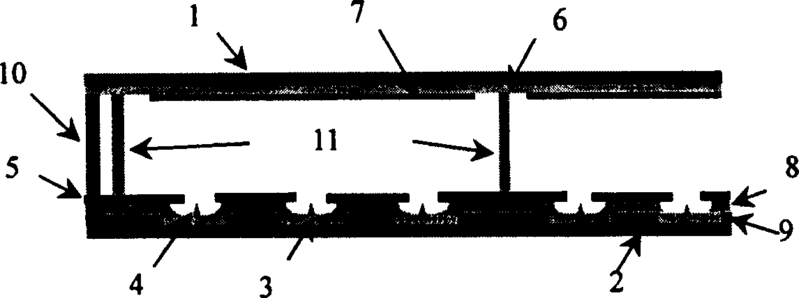
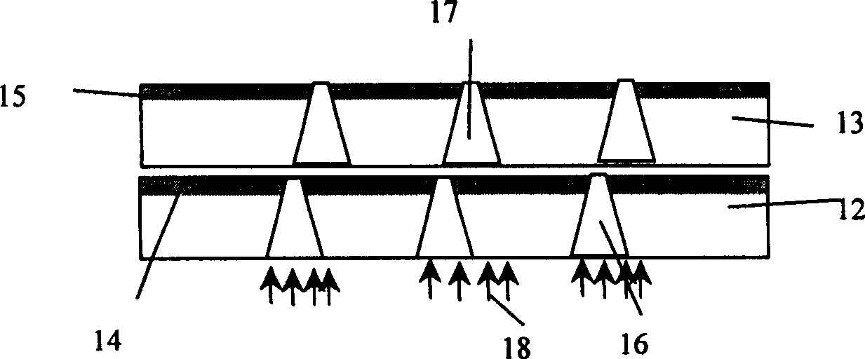
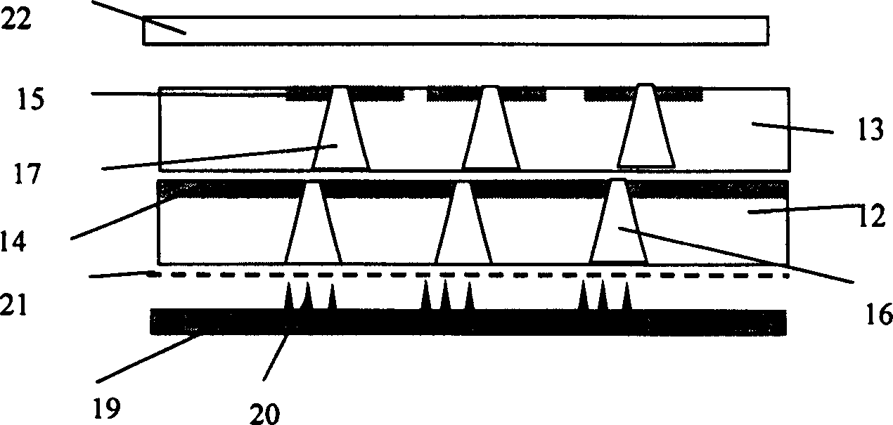
[0013] The field emission addressing structure with low modulation voltage dynamic range of the present invention is composed of a dielectric plate and a dielectric layer, and is characterized in that the structure is composed of an upper dielectric plate 13 and a lower dielectric plate 12 stacked together, and the upper dielectric plate 13 is provided with an upper medium tapered hole 17, a lower medium tapered hole 16 is provided on the lower medium plate 12, and a modulation electrode 15 is provided on the upper surface of the upper medium plate 13, that is, the small hole end of the upper medium tapered hole 17, The upper surface of the lower dielectric flat plate 12, that is, the small hole end of the lower dielectric tapered hole 16, is provided with an addressing electrode 14, wherein the upper dielectric tapered hole 17 on the upper dielectric flat plate 13 and the lower dielectric tapered hole on the lower dielectric flat plate 12 The center line of 16 is not on the sa...


PUM


Abstract

The field emission addressing structure with low modulation voltage dynamic range relates to field emission display devices, especially the structure for realizing low modulation voltage dynamic range by changing the structure of field emission devices. The structure consists of an upper medium plate (13) and a lower medium plate (12) stacked together, the upper medium plate is provided with an upper medium tapered hole (17), and the lower medium plate is provided with a lower medium tapered hole (16), on the upper surface of the upper dielectric plate, that is, the aperture end of the upper medium tapered hole is provided with a modulation electrode (15), and on the upper surface of the lower dielectric plate, that is, the aperture end of the lower medium tapered hole is provided with an addressing electrode (14), wherein the centerlines of the upper medium tapered hole on the upper medium plate and the lower medium tapered hole on the lower medium plate are not on the same center line, the invention provides a low field emission display screen modulation voltage seeker The field emission addressing structure with low modulation voltage dynamic range achieves the purpose of low modulation voltage addressing by controlling the migration of secondary electrons on the surface of the medium.

Description

technical field [0001] The invention relates to a field emission display device, especially a structure for realizing a low modulation voltage dynamic range by changing the structure of the field emission device. Background technique [0002] At present, it is a hot spot in the development of flat panel displays. At present, there are more researches on flat panel displays, such as liquid crystal display, plasma display, field emission display, etc., because liquid crystal display is passive light emitting, so the brightness is low, and at the same time, it has small viewing angle and slow response speed. Plasma display has large size display, but it has certain difficulties in luminous efficiency and high resolution display; field emission display is a cold cathode emission, active light-emitting flat panel display device, with high luminous brightness and low power consumption , large viewing angle, suitable for high-resolution display, etc., so the research on field emiss...

Claims


Application Information

Patent Timeline
IPC IPC(8): H01J29/46H01J31/12
Inventor 雷威张晓兵
Owner SOUTHEAST UNIV
Why Eureka
Try Eureka