
Method for mfg. semiconductor device with element separating insulation film

A technology for component separation and manufacturing method, which is applied in semiconductor/solid-state device manufacturing, semiconductor devices, electrical components, etc., and can solve the problems of short circuit of etching residues, deep level difference problems, and messing up the impurity concentration on the surface of the substrate.

Inactive Publication Date: 2004-09-08
RENESAS ELECTRONICS CORP
View PDF1 Cites 0 Cited by
  • Summary
  • Abstract
  • Description
  • Claims
  • Application Information

AI Technical Summary

Problems solved by technology

For the latter, the following level difference problem becomes profound
[0013] The second problem is that the reduction of the element isolation oxide film by wet etching from the initial oxidation state will cause a step difference at the boundary between the diffusion layer and the element isolation oxide film, and cause short circuits due to the etch residue of the gate electrode.
[0014] The third problem is that, as a result of repeatedly oxidizing the substrate surface and then removing it by wet etching, the impurity concentration on the substrate surface is disturbed, making the electrical characteristics (especially the threshold value of the triode) unstable
[0015] The fourth problem is that due to the repeated oxidation and wet etching of the substrate surface, the surface roughness is increased and the electrical characteristics are deteriorated.
[0016] Such a disadvantage is caused by the formation of an oxide film that is unnecessary for the element

Method used


Image

  • Method for mfg. semiconductor device with element separating insulation film
  • Method for mfg. semiconductor device with element separating insulation film
  • Method for mfg. semiconductor device with element separating insulation film

Examples


Embodiment Construction

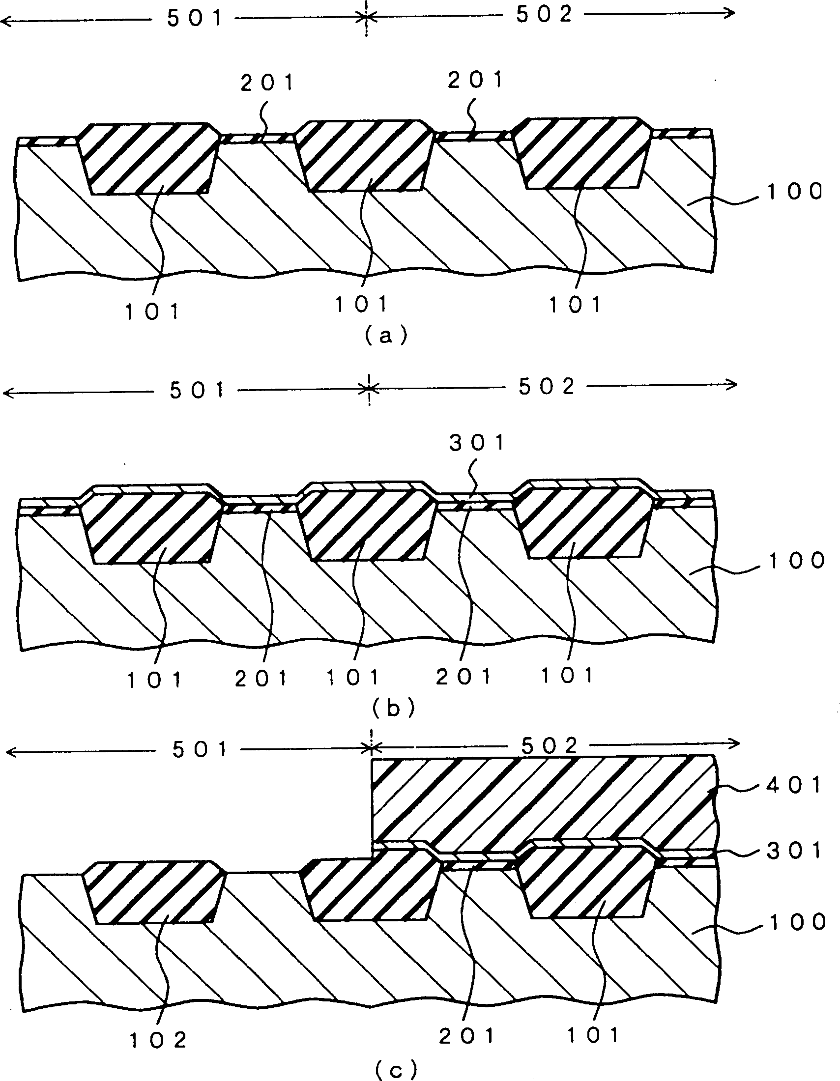
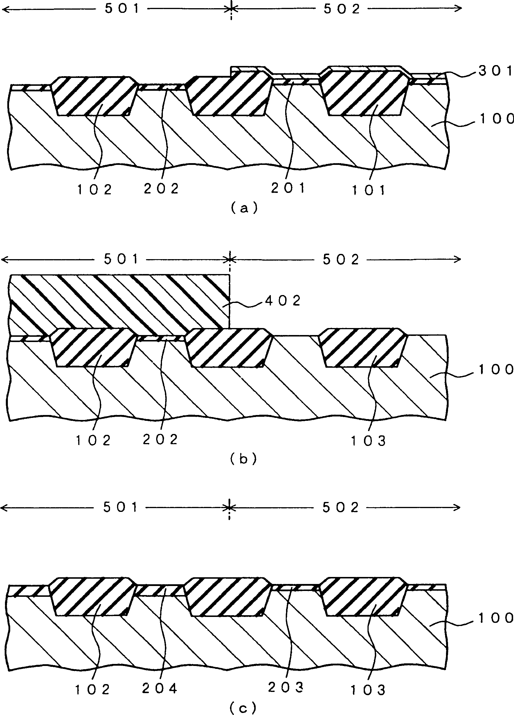
[0030] Hereinafter, a method of manufacturing a semiconductor device having an element isolation insulating film according to an embodiment of the present invention will be specifically described with reference to the drawings. figure 1 (a)~(c) and figure 2 (a) to (c) are cross-sectional views showing the sequence of steps of a method of manufacturing a semiconductor device having an element isolation insulating film according to Embodiment 1 of the present invention.

[0031] figure 1 (a) shows the element isolation insulating film 101 formed on the surface of the silicon substrate 100 to electrically isolate elements, and the thin oxide film 201 formed to protect the substrate during ion implantation in the active region sandwiched by the element isolation insulating film 101 cross-sectional view of the state. As shown in the figure, the silicon substrate 100 has an element region 501 that requires a thick gate oxide film for a high withstand voltage circuit such as a w...


PUM


Abstract

The present invention relates to a manufacturing method for a semi-conductive device with element isolation. There is anti-oxidation film 301 formed on the total surface of the semiconductor base plates 100 of element domains 501 and 502 on which there are many element separate oxide films 101 and thin oxide film 201 on the active domain formed. After semiconductor base plate 100 of element domain 501 masks the developed resistant film 401 is developed, the first gate oxide film is formed. And the semiconductor base plate 100 of element domain 502 masks the opened resistant film 401 is further developed, the second gate oxidation is carrying on. It avoids that there is unnecessary oxide film formed on the base plate so as to reduce the steps of etching before gate oxidation.

Description

technical field [0001] The present invention relates to a method of manufacturing a semiconductor device having an element isolation insulating film, and more particularly to a method for forming a different gate oxide film on the same chip by using a nitride film or the like before gate oxidation. A semiconductor device manufacturing method of an element isolation insulating film that covers each element region with an oxidation-resistant film to improve the reliability of the element, especially the element isolation characteristic. Background technique [0002] Generally, in a MOS semiconductor device equipped with an insulated gate field effect transistor (MOS transistor), it is necessary to have a high withstand voltage element with high withstand voltage reliability and a low withstand voltage element for high-speed information processing in the same semiconductor device. In the case of devices, it is necessary to increase the thickness of the gate oxide film and the f...

Claims


Application Information

Patent Timeline
Patent Type & Authority Patents(China)
IPC IPC(8): H01L21/762H01L21/316H01L21/76H01L21/8234H01L27/088
CPCH01L21/823481H01L21/823462H01L21/76
Inventor 清水正邦
Owner RENESAS ELECTRONICS CORP
Learn More