Substrate layer-adding processing method and packaging structure

A processing method and substrate technology, applied in semiconductor/solid-state device parts, semiconductor devices, electrical components, etc., can solve the problem that the amount of thinning cannot be accurately controlled, and achieve stability and performance, and reduce the feed speed of the grinding wheel Effect

Pending Publication Date: 2022-08-05
WUXI ZHONGWEI GAOKE ELECTRONICS
View PDF0 Cites 0 Cited by
  • Summary
  • Abstract
  • Description
  • Claims
  • Application Information

AI Technical Summary

Problems solved by technology

[0003] The invention provides a substrate build-up processing method and packaging structure, which solves the problem that the amount of thinning cannot be precisely controlled in the related art

Method used


Image

  • Substrate layer-adding processing method and packaging structure
  • Substrate layer-adding processing method and packaging structure
  • Substrate layer-adding processing method and packaging structure

Examples


Embodiment Construction

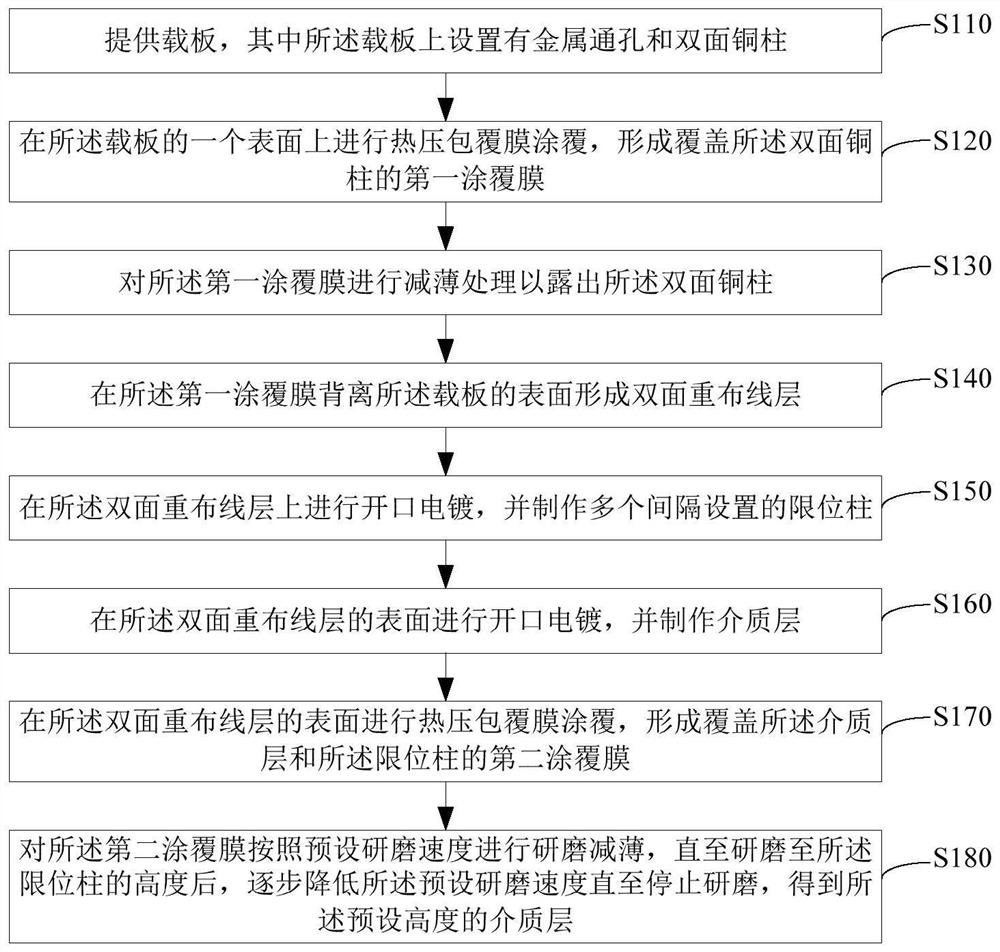
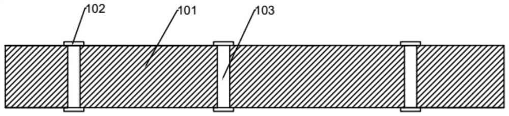
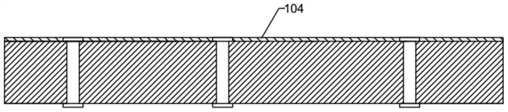
[0031] It should be noted that the embodiments of the present invention and the features of the embodiments may be combined with each other under the condition of no conflict. The present invention will be described in detail below with reference to the accompanying drawings and in conjunction with the embodiments.

[0032] In order for those skilled in the art to better understand the solutions of the present invention, the technical solutions in the embodiments of the present invention will be clearly and completely described below with reference to the accompanying drawings in the embodiments of the present invention. Obviously, the described embodiments are only Embodiments of some, but not all, of the present invention. Based on the embodiments of the present invention, all other embodiments obtained by persons of ordinary skill in the art without creative efforts shall fall within the protection scope of the present invention.

[0033] It should be noted that the terms ...


PUM

PropertyMeasurementUnit
diameteraaaaaaaaaa
heightaaaaaaaaaa
thicknessaaaaaaaaaa

Abstract

The invention relates to the technical field of semiconductor processing technologies, and particularly discloses a substrate layer-adding processing method which comprises the following steps: providing a carrier plate; hot-pressing coating film coating is conducted on one surface of the carrier plate, and a first coating film covering the double-face copper columns is formed; thinning the first coating film to expose the double-sided copper column; forming a double-sided rewiring layer on the surface, deviating from the carrier plate, of the first coating film; manufacturing a plurality of spaced limiting columns on the double-sided rewiring layer, wherein the mechanical property parameters of the manufacturing material of the limiting columns meet the following conditions: the Mohs hardness is greater than 3.0, the Young modulus is greater than 110 GPa, and the shear elastic modulus is greater than 49 GPa; opening electroplating is carried out on the surface of the double-sided rewiring layer, and a dielectric layer is manufactured; and performing hot-pressing coating film coating on the surface of the double-sided rewiring layer to form a second coating film covering the dielectric layer and the limiting columns. The invention also discloses a packaging structure. According to the substrate layer-adding processing method provided by the invention, the thinning thickness can be effectively controlled.

Description

technical field [0001] The invention relates to the technical field of semiconductor processing technology, in particular to a substrate build-up processing method and a packaging structure. Background technique [0002] FC-BGA (Flip Chip-Ball Grid Array, Flip Chip Ball Grid Array packaging format) substrate build-up technology is to use drilling, hole plating and hole filling technology to conduct layer-to-layer conduction on the coating film , and prepare a single-layer circuit layer on it to realize the connection of the circuit. At the same time, it is also possible to make the circuit layer and then hot-press the film to fill the entire circuit layer. However, this is in the medium filled between the metal layers. The thickness of the material is carried out under the premise that the thickness of the material conforms to the theoretical thickness. At present, the thickness of the coating film is larger than the theoretical thickness of the dielectric layer, and after t...

Claims


Application Information

Patent Timeline
Patent Type & Authority Applications(China)
IPC IPC(8): H01L21/48H01L23/498
CPCH01L21/4846H01L23/498
Inventor 李轶楠李明姚昕靳学昌
Owner WUXI ZHONGWEI GAOKE ELECTRONICS
Why Eureka
Try Eureka