Wafer clamping device

A clamping device and chip technology, which is applied in the manufacture of electrical components, circuits, semiconductors/solid-state devices, etc., can solve problems such as difficulty in taking chips, and achieve the effects of overcoming electrostatic attraction, reducing influence, and improving uniformity

Pending Publication Date: 2022-07-22
BEIJING SHUOKE ZHONGKEXIN ELECTRONICS EQUIP CO LTD
View PDF0 Cites 0 Cited by
  • Summary
  • Abstract
  • Description
  • Claims
  • Application Information

AI Technical Summary

Problems solved by technology

Due to its unique piezoelectric characteristics and pyroelectric effect, lithium lithium oxide and other piezoelectric crystal materials often form static electricity on the surface of the wafer during the process. This surface static electricity will form an attractive force between the wafer backplanes, and the wafer will be adsorbed To the backplane, it is difficult to take the chip, or even fragments. In the current two clamping methods, there is a problem of how to release or eliminate the static electricity on the wafer surface

Method used


Image

  • Wafer clamping device
  • Wafer clamping device
  • Wafer clamping device

Examples


Embodiment Construction

[0031] The present invention will be described in detail below with reference to the accompanying drawings and in conjunction with the embodiments. It should be noted that the embodiments of the present invention and the features of the embodiments may be combined with each other under the condition of no conflict. For the convenience of description, the words "up", "down", "left" and "right" appear in the following text, which only means that the directions of up, down, left and right are consistent with the drawings themselves, and do not limit the structure.

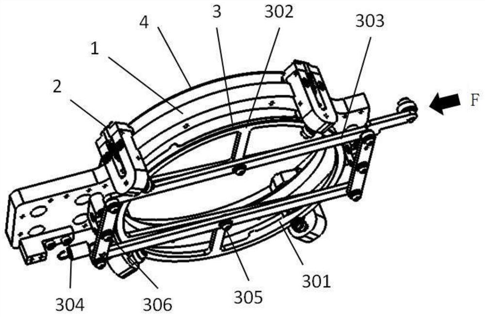
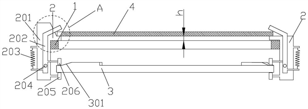
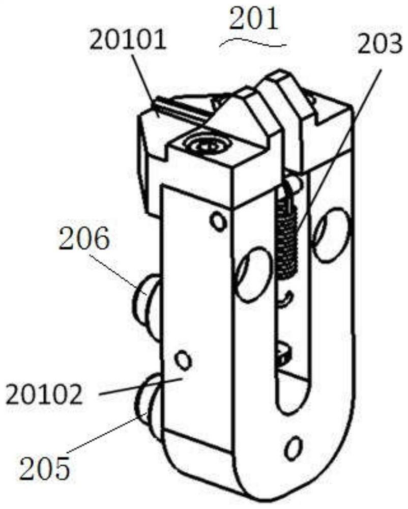
[0032] like figure 1 As shown, a wafer clamping device provided in this embodiment includes a substrate 1 , a fixing unit 2 and an unlocking mechanism 3 .

[0033] like figure 1 , figure 2 As shown, the substrate 1 is made of aluminum alloy and has a cavity that matches the size of the wafer 4 to form a hollow annular plate. The substrate 1 is the base of the wafer holding device. Four fixing units 2 are arrange...


PUM


Abstract

The invention provides a wafer clamping device. The wafer clamping device comprises a base plate, fixing units and an unlocking mechanism, at least three fixing units are arranged on the periphery of the base plate, a certain distance h is kept between a supporting wafer and the base plate, one side of the base plate is provided with the unlocking mechanism, and the other side of the base plate is provided with an installation space used for containing the wafer; and the unlocking mechanism moves relative to one end of the fixing unit, so that the other end of the fixing unit gets close to the mounting space for clamping or gets away from the mounting space for loosening. According to the method, the influence of the electrostatic attraction on the back surface of the wafer is overcome, meanwhile, a way is provided for eliminating static electricity, and the problem that the wafer is difficult to take due to the static electricity generated in the injection process of the lithium acid lithium wafer and the like is solved.

Description

technical field [0001] The present invention relates to the technical field of semiconductors, and in particular, to a wafer clamping device. Background technique [0002] At present, the existing wafer clamping generally includes mechanical clamping and electrostatic clamping. These two clamping methods generally have a solid structure on the back of the wafer in contact with the wafer. The mechanical clamping is generally a water-cooled backplane, and the electrostatic clamping is generally There is a water-cooled backplane and an insulating layer. Due to its unique piezoelectric properties and pyroelectric effect, piezoelectric crystal materials such as lithium lithium oxide often form static electricity on the surface of the wafer during the process. This surface static electricity will form an attractive force between the wafer backplanes and adsorb the wafer To the backplane, it leads to difficulty in taking wafers, and even debris. In the current two clamping methods...

Claims


Application Information

Patent Timeline
IPC IPC(8): H01L21/687
CPCH01L21/68714H01L21/68785H01L21/68721
Inventor 彭立波胡旭波易镓
Owner BEIJING SHUOKE ZHONGKEXIN ELECTRONICS EQUIP CO LTD
Why Eureka
Try Eureka