PCB welding device

A technology for welding devices and PCB boards, which is applied in the direction of assembling printed circuits, printed circuits, and electrical components with electrical components, and can solve problems such as inability to perform normal work, decline in welding quality, and waste of solder, so as to avoid the decline in welding quality and increase Brightness, reduce the effect of raw material loss

Pending Publication Date: 2022-07-12
安徽宏鑫电子科技有限公司
View PDF0 Cites 0 Cited by
  • Summary
  • Abstract
  • Description
  • Claims
  • Application Information

AI Technical Summary

Problems solved by technology

[0003] In order to overcome the above-mentioned technical problems, the object of the present invention is to provide a PCB board welding device, which can carry out surface treatment on the PCB board, and solve the obvious black boundary between the solder and the lead wire of the component or the copper foil due to the untreated surface. , The solder is sunken to the boundary, the problem of not being able to work normally, and the problem of solder waste caused by too much spraying solution and the decline of soldering quality

Method used


Image

  • PCB welding device
  • PCB welding device
  • PCB welding device

Examples


Embodiment Construction

[0023] The technical solutions in the embodiments of the present invention will be clearly and completely described below with reference to the accompanying drawings in the embodiments of the present invention. Obviously, the described embodiments are only a part of the embodiments of the present invention, rather than all the embodiments. Based on the embodiments of the present invention, all other embodiments obtained by those of ordinary skill in the art without creative efforts shall fall within the protection scope of the present invention.

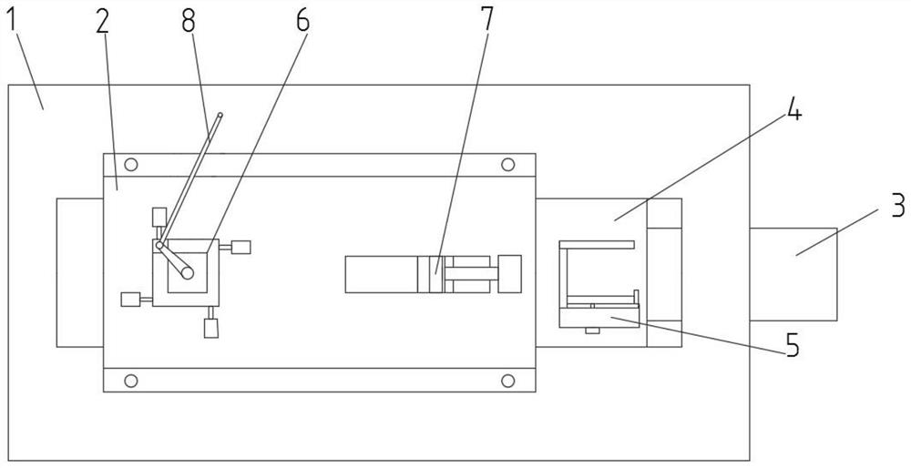
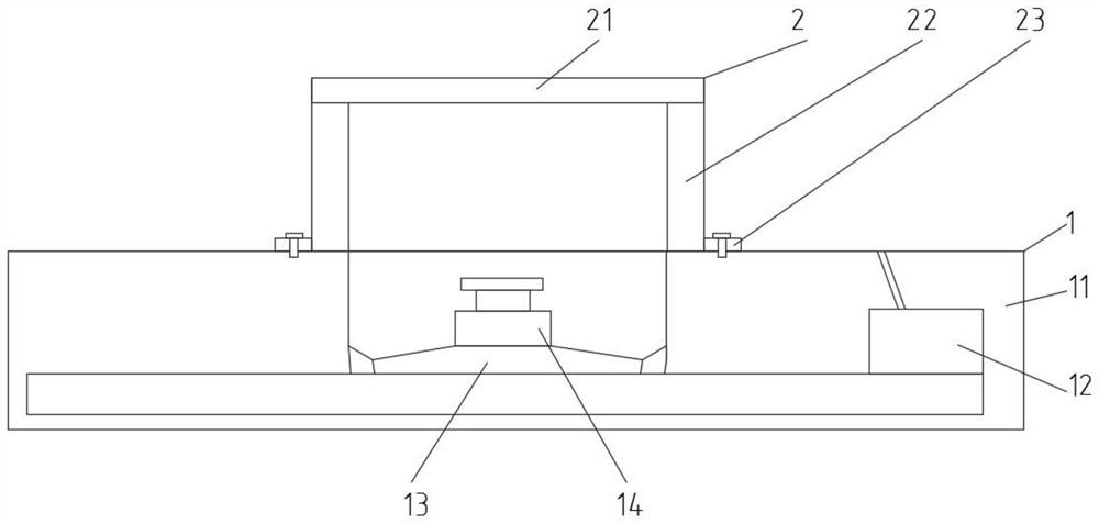
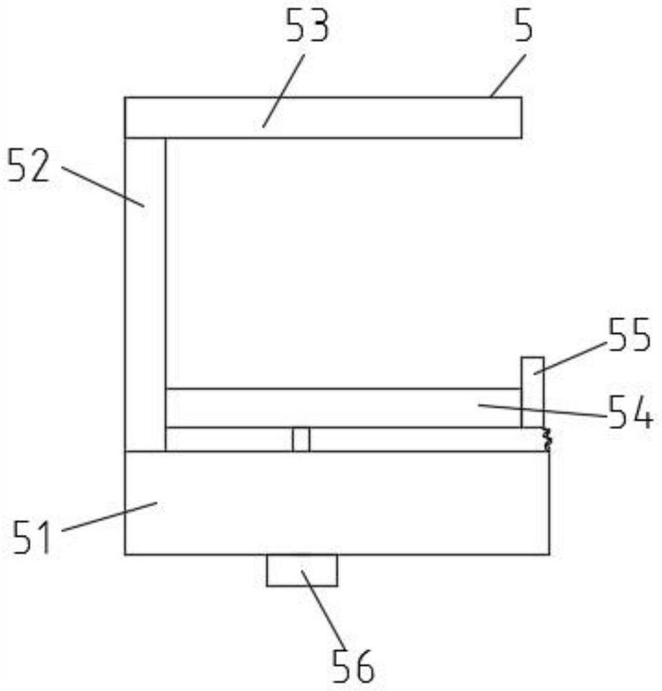
[0024] see Figure 1-6As shown, a PCB board welding device includes a fixing mechanism 1, an installation mechanism 2, a material guide plate 3 and a belt conveyor 4. The belt conveyor 4 is an existing equipment, and will not be repeated here. The conveyor 4 is installed inside the groove provided on the upper surface of the fixing mechanism 1, the installation mechanism 2 is screwed on the upper end of the fixing mechanism 1, the ma...


PUM


Abstract

The invention discloses a PCB welding device which comprises a fixing mechanism, a mounting mechanism, a guide plate and a belt conveyor, the belt conveyor is an existing device, excessive details are not needed, the belt conveyor is mounted in a groove formed in the upper surface of the fixing mechanism, the mounting mechanism is connected to the upper end of the fixing mechanism in a threaded mode, and the guide plate is connected to the fixing mechanism in a threaded mode. The material guide plate is located on one side of the fixing mechanism, one end of the material guide plate extends into the groove, the other end of the material guide plate is located below the belt conveyor, a plurality of clamping mechanisms arranged at equal intervals are installed on the outer surface of the belt conveyor, and the belt conveyor is used for conveying the clamping mechanisms; the device is used for conducting pre-welding treatment on the PCB, and the problems that due to the fact that the surface is not treated thoroughly, an obvious black boundary exists between soldering tin and a component lead or between the soldering tin and a copper foil, the soldering tin sinks towards the boundary, normal work cannot be conducted, and the problems that welding flux is wasted and welding quality is reduced due to the fact that too much solution is sprayed are solved.

Description

technical field [0001] The invention relates to the technical field of surface treatment before PCB board welding, in particular to a PCB board welding device. Background technique [0002] PCB, the Chinese name is printed circuit board, also known as printed circuit board, is an important electronic component, a support body for electronic components, and a carrier for electrical connection of electronic components. Because it is made by electronic printing, it is called "printed" circuit board, and the printed board has developed from single layer to double-sided and multi-layer, and still maintains its own development trend. Due to the continuous development in the direction of high precision, high density and high reliability, continuous reduction in size, cost reduction and performance improvement, the printed board still maintains a strong vitality in the development process of electronic equipment in the future. Due to its welding quality Due to the high requirements...

Claims


Application Information

Patent Timeline
Patent Type & Authority Applications(China)
IPC IPC(8): H05K3/00H05K3/26H05K3/34
CPCH05K3/0011H05K3/26H05K3/34H05K2203/0257H05K2203/048H05K2203/0485H05K2203/15H05K2203/17Y02P70/10
Inventor 陈世杰
Owner 安徽宏鑫电子科技有限公司
Why Eureka
Try Eureka