


Quick Research
Generate reliable direction feasibility study reports for your R&D in just a few steps.

Technical Q&A
Discover and master advanced knowledge NOW. Basics, ideas, possibilities, all at once.

Find Solutions
As an expert in R&D theories, this can generate solutions to your technical problems instantly.

Evaluate Feasibility
Analyze your overall solution with one click, know your potential R&D risks in advance.

Monitor Landscape
Get weekly tech updates, stay abreast of the latest tech innovations and key insights.
Method for preparing stable CsPbI2Br inorganic perovskite thin film based on high-flux gas phase co-evaporation
A high-throughput, inorganic calcium technology, applied in the direction of electrical components, vacuum evaporation plating, coating, etc., can solve the problems of irreversible degradation of perovskite, to facilitate photocurrent transmission, improve device efficiency, and improve photoelectric conversion efficiency effect
- Summary
- Abstract
- Description
- Claims
- Application Information
AI Technical Summary
Problems solved by technology
Method used
Image

Examples
Embodiment 1
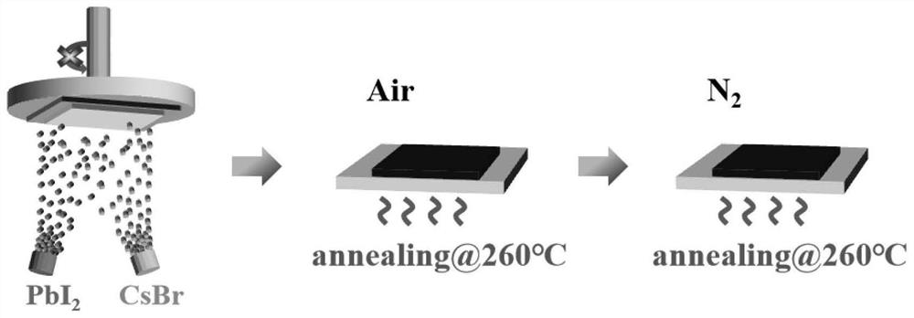
[0034] This example provides the preparation of stable CsPbI based on high-throughput gas-phase co-evaporation 2 methods for Br inorganic perovskite thin films, such as figure 1 shown, including the following steps:
[0035] Step 1. Select 2×2cm transparent electronic grade glass as the substrate, first use deionized water to rinse the substrate several times, and then use deionized water, acetone, and ethanol as the solvent to perform ultrasonic treatment on the rinsed substrate in turn. 10 minutes; the ultrasonically treated substrate is blown dry with nitrogen gas, and then treated with oxygen plasma to enhance the bonding force and adhesion on the surface of the substrate material;
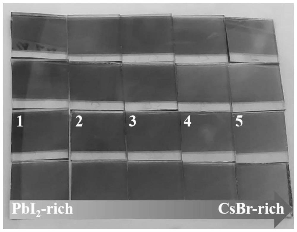
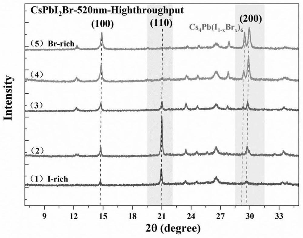
[0036] Step 2. Arrange 4×5 substrates processed in step 1 closely in the middle of the sample holder of the evaporation chamber in a rectangular array, and the size of the sample holder is 14×12 cm; put the evaporation source cesium bromide (see figure 1 the left evaporation source) and lead i...
Embodiment 2
[0045] This embodiment provides a stable CsPbI-based 2 Br inorganic perovskite thin films for perovskite solar cells, such as Figure 5 As shown, including transparent conductive glass (that is, glass substrate with transparent conductive electrodes attached), electron transport layer, stabilized CsPbI arranged in sequence from bottom to top 2 Br inorganic perovskite thin films, hole transport layers and metal electrodes.
[0046] Among them, the electron transport layer is TiO 2 Dense layer, 40 nm thick; stabilized CsPbI 2 The thickness of the Br perovskite thin film is 400 nm; the hole transport layer is a Spiro-OMeTAD layer with a thickness of 150 nm; the metal electrode is a gold electrode with a thickness of 100 nm.
[0047] The above is based on stable CsPbI 2 The preparation method of the perovskite solar cell of the Br inorganic perovskite thin film includes the following steps:
[0048] Step 1. Select 2 × 2cm transparent conductive glass as the substrate, first u...
PUM
| Property | Measurement | Unit |
|---|---|---|
| Thickness | aaaaa | aaaaa |
| Thickness | aaaaa | aaaaa |
| Thickness | aaaaa | aaaaa |
Abstract
Description
Claims
Application Information
 - R&D Engineer
- R&D Manager
- IP Professional
- Industry Leading Data Capabilities
- Powerful AI technology
- Patent DNA Extraction
Browse by: Latest US Patents, China's latest patents, Technical Efficacy Thesaurus, Application Domain, Technology Topic, Popular Technical Reports.
© 2024 PatSnap. All rights reserved.Legal|Privacy policy|Modern Slavery Act Transparency Statement|Sitemap|About US| Contact US: help@patsnap.com