Substrate for testing flat panel detector and testing method thereof
A technology of flat-panel detectors and substrates, applied in semiconductor/solid-state device testing/measurement, semiconductor devices, electric solid-state devices, etc., can solve the problem of TFT characteristic difference between Teg area and AA area, and avoid inaccurate test data, The effect of good characteristics and fast response speed of the test
- Summary
- Abstract
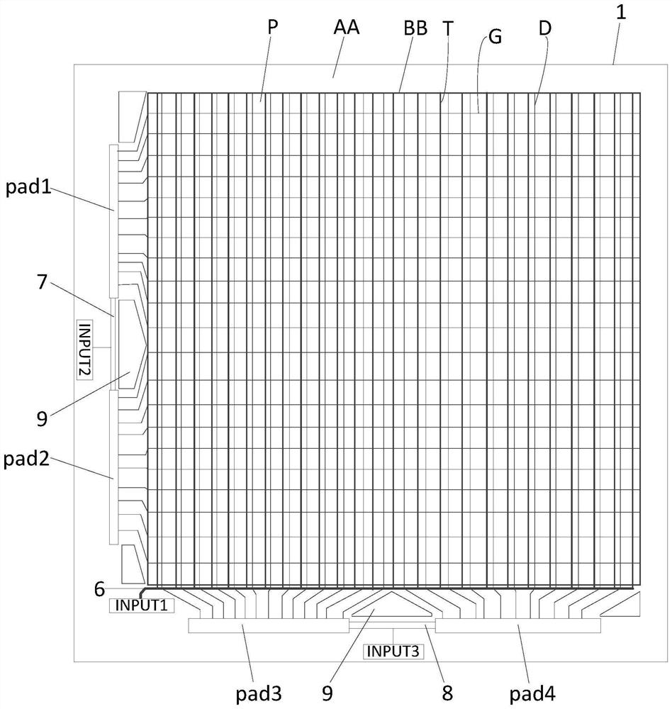
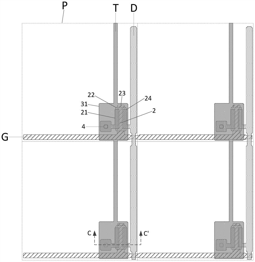
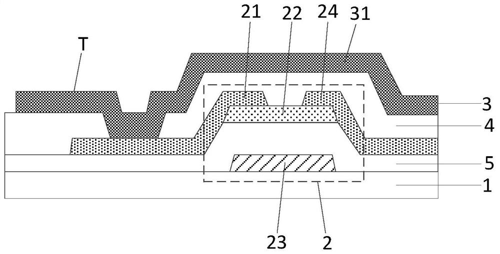
- Description
- Claims
- Application Information
AI Technical Summary
Problems solved by technology
Method used
Image

Examples
Embodiment Construction
[0027] To make the objectives, technical solutions and advantages of the embodiments of the present invention clearer, the technical solutions of the embodiments of the present invention will be clearly and completely described below with reference to the accompanying drawings of the embodiments of the present invention. Obviously, the described embodiments are some, but not all, embodiments of the present invention. Also, the embodiments of the present invention and the features of the embodiments may be combined with each other without conflict. Based on the described embodiments of the present invention, all other embodiments obtained by those of ordinary skill in the art without creative work fall within the protection scope of the present invention.
[0028] Unless otherwise defined, technical or scientific terms used in the present invention shall have the ordinary meaning as understood by one of ordinary skill in the art to which the present invention belongs. When use...
PUM
 Abstract
Description
Claims
Application Information
 - Generate Ideas
- Intellectual Property
- Life Sciences
- Materials
- Tech Scout
- Unparalleled Data Quality
- Higher Quality Content
- 60% Fewer Hallucinations
Browse by: Latest US Patents, China's latest patents, Technical Efficacy Thesaurus, Application Domain, Technology Topic, Popular Technical Reports.
© 2025 PatSnap. All rights reserved.Legal|Privacy policy|Modern Slavery Act Transparency Statement|Sitemap|About US| Contact US: help@patsnap.com