Die bonding structure and die bonding process
A technology of solid crystal and process, applied in the direction of semiconductor devices, electrical components, circuits, etc., can solve the problems of low reflectivity of ceramic plates and unsatisfactory light brightness, etc., to increase reflectivity, increase heat conduction channels, and improve thermal conductivity Effect
- Summary
- Abstract
- Description
- Claims
- Application Information
AI Technical Summary
Problems solved by technology
Method used
Image
Examples
Embodiment 1
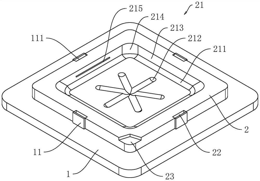
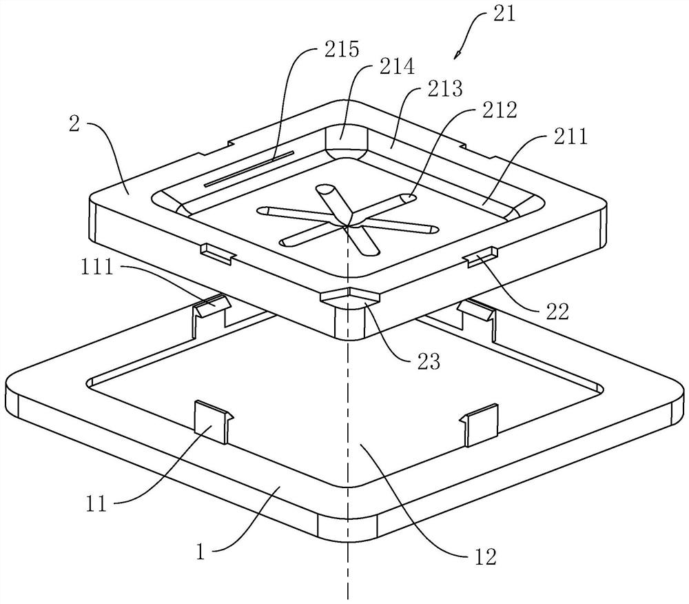
[0056] refer to figure 1 , the top corner of the substrate 2 is provided with a diagonal groove 23, the function of the diagonal groove 23 is to facilitate the subsequent installation of the LED bracket, and provide a function of positioning the installation direction of the LED bracket, thereby ensuring the accuracy of the installation of the LED bracket.
[0057] refer to figure 1 and figure 2 A sunken groove 21 is provided on the top surface of the substrate 2 away from the base 1. The groove 21 includes a crystal-bonding area for bonding LED chips and a reflection area for increasing the reflection area. The difference between the reflection area and the crystal-bonding area is A first arc-shaped surface 211 is provided at the junction between them. The function of the first arc-shaped surface 211 is to increase the reflective area while enabling a smooth transition of the die-bonding glue between the reflective area and the die-bonding area, reducing the risk of die-bon...
Embodiment 2
Embodiment 3
PUM
 Abstract
Description
Claims
Application Information
 - R&D Engineer
- R&D Manager
- IP Professional
- Industry Leading Data Capabilities
- Powerful AI technology
- Patent DNA Extraction
Browse by: Latest US Patents, China's latest patents, Technical Efficacy Thesaurus, Application Domain, Technology Topic, Popular Technical Reports.
© 2024 PatSnap. All rights reserved.Legal|Privacy policy|Modern Slavery Act Transparency Statement|Sitemap|About US| Contact US: help@patsnap.com


