Mask for partial plating, method for manufacturing insulated circuit board using said mask, and partial plating method
A technology of insulating substrates and circuit substrates, which is applied in the fields of printed circuit manufacturing, printed circuit components, circuits, etc., can solve problems not specifically disclosed, and achieve the effects of improving productivity, reducing costs, and simple structure
- Summary
- Abstract
- Description
- Claims
- Application Information
AI Technical Summary
Problems solved by technology
Method used
Image
Examples
Embodiment 1
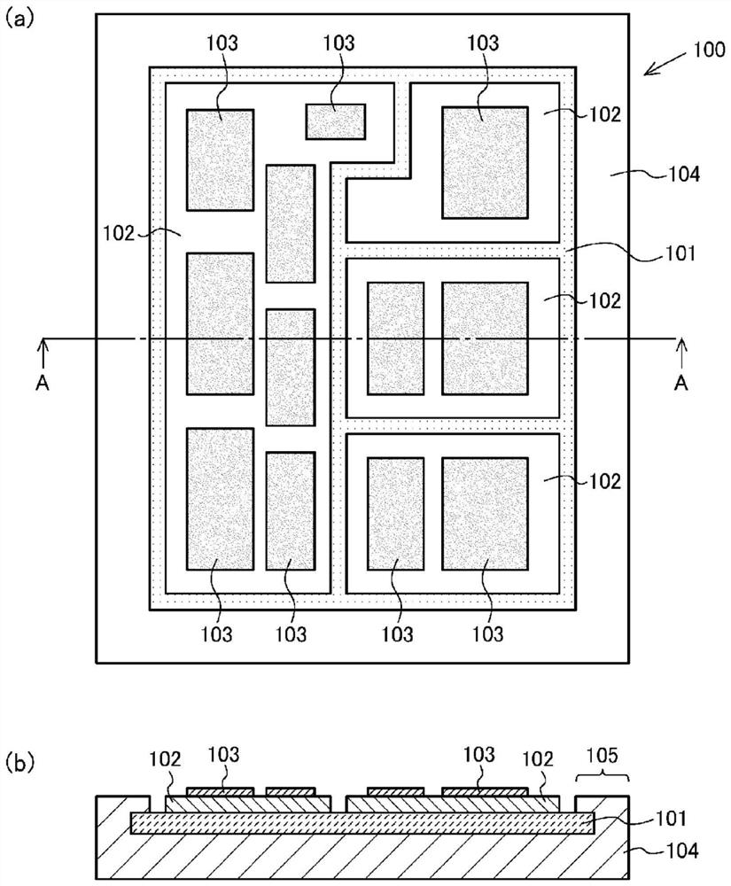
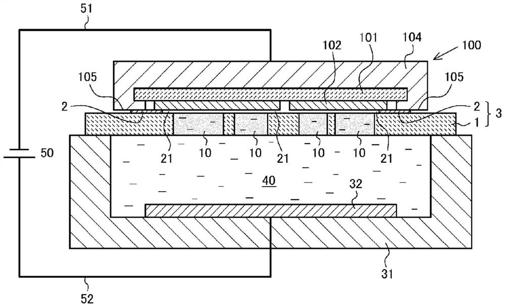
[0094] ready to have with figure 1 The example shown is an insulating circuit board with the same laminated structure (however, the plating layer has not been formed yet). metal parts ( figure 1 The configuration of symbol 102) is also with figure 1 similar. The islands of the metal component are respectively electrically isolated on the insulating substrate. insulating substrate ( figure 1 The symbol 101) is an aluminum nitride plate with a size of 67mm×71mm×0.6mm. Metal parts to be joined on ( figure 1 The symbol 102) is a plate with a thickness of 1.3mm made of pure aluminum with a purity of 99.9%. The heat dissipation base bonded to the back of the insulating substrate ( figure 1 The symbol 104) is also made of pure aluminum with a purity of 99.9%, and has a peripheral wall portion ( figure 1 symbol 105). The thickness of the heat dissipation base was 3 mm in the back portion of the insulating substrate. In addition, the aluminum nitride plate, the metal m...
Embodiment 2
[0101] Ni plating was performed on a predetermined portion of the insulating circuit board under the same conditions as in Example 1 except that a conductive silicone rubber sheet was used as the conductive sheet member. The volume resistivity of this conductive silicone rubber sheet was 10 Ω·cm. When the insulating circuit board after plating was observed, bleeding was not seen at all, and plating with high dimensional accuracy was realized.
[0102] In addition, when a conductive silicone rubber sheet is used as the conductive sheet member, the liquid leakage prevention effect is high, so the conductive sheet member is less likely to react with the plating solution. Since the conductive silicone rubber sheet is inexpensive, it has the advantage of being able to prolong its life without using an expensive titanium plate.
Embodiment 3
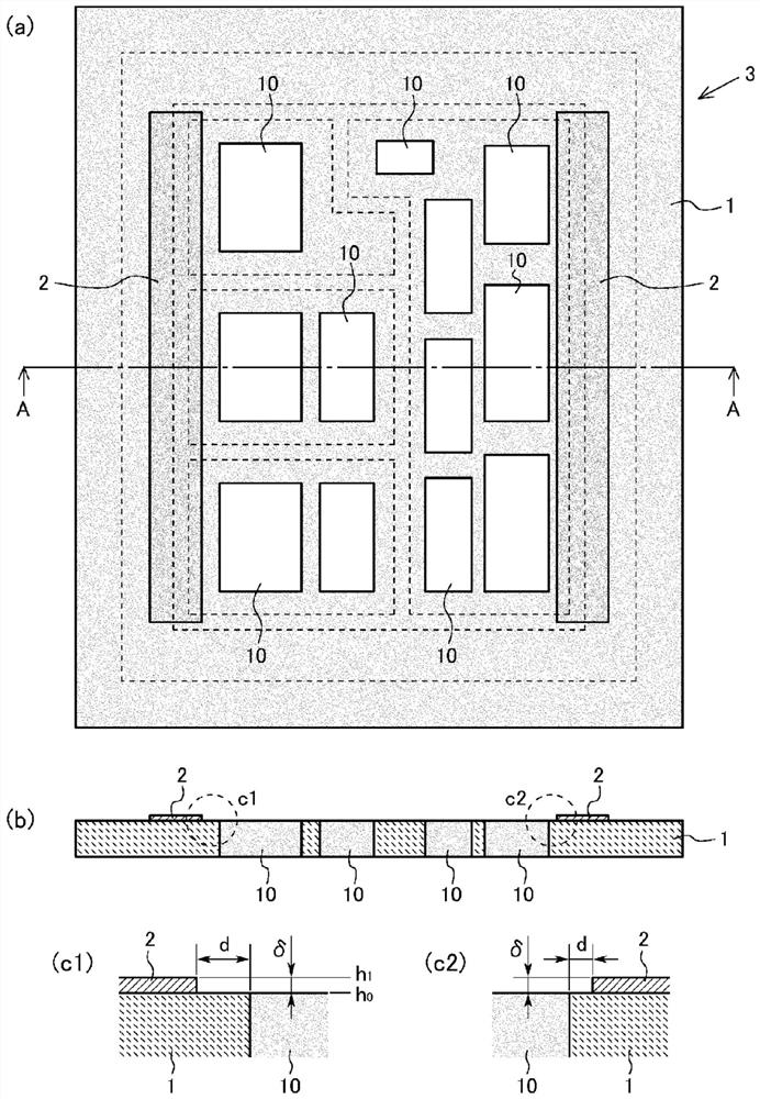
[0104] As a mask for partial plating, instead of the type in which a conductive sheet part is embedded in a concave part of an insulating sheet part, such as figure 2 The shown type is a type in which a conductive sheet member is pasted on the surface of a flat insulating sheet member without recesses. In addition, the material of the conductive sheet member was SUS304, and the thickness thereof was 0.01 mm. Except for this, in the same manner as in Example 1, Ni plating was performed on a predetermined portion of the insulating circuit board.
[0105] The thickness of the insulating sheet member of the partial plating mask was 4 mm. The volume resistivity of the SUS304 plate used as the conductive sheet member was 72 µΩ·cm. The arrangement of the conductive sheet member and the arrangement of the openings of the plating mask partially viewed in the thickness direction are the same as in Example 1. Therefore, the distance d from the end of the conductive sheet member to the...
PUM
| Property | Measurement | Unit |
|---|---|---|
| thickness | aaaaa | aaaaa |
| depth | aaaaa | aaaaa |
| width | aaaaa | aaaaa |
Abstract
Description
Claims
Application Information
 - R&D
- Intellectual Property
- Life Sciences
- Materials
- Tech Scout
- Unparalleled Data Quality
- Higher Quality Content
- 60% Fewer Hallucinations
Browse by: Latest US Patents, China's latest patents, Technical Efficacy Thesaurus, Application Domain, Technology Topic, Popular Technical Reports.
© 2025 PatSnap. All rights reserved.Legal|Privacy policy|Modern Slavery Act Transparency Statement|Sitemap|About US| Contact US: help@patsnap.com


