Thin film solar cell and preparation method thereof
A technology of thin-film solar cells and ferroelectric films, applied in circuits, photovoltaic power generation, electrical components, etc., can solve the problem of difficult to achieve effective separation of photo-generated carriers, efficient transfer of charges, inability to provide CIGS photo-generated carriers with efficient transfer, and short-circuit current Low density and other issues, achieve high visible light transmittance, improve separation and transmission capabilities, and good electrical conductivity
- Summary
- Abstract
- Description
- Claims
- Application Information
AI Technical Summary
Problems solved by technology
Method used
Image
Examples
preparation example Construction
[0040] The present invention also provides a method for preparing a thin-film solar cell described in the above technical solution, comprising the following steps:
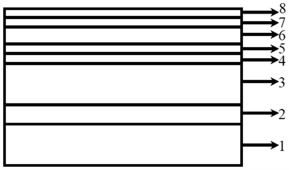
[0041] A first carrier transport layer, a p-type optical absorption layer, an n-type window layer, a magnetron sputtering ferroelectric film layer, a second carrier transport layer and a metal gate electrode layer are sequentially prepared on the substrate.
[0042] Before preparing the first carrier transport layer on the substrate, the present invention preferably cleans the substrate. In the present invention, there is no special limitation on the cleaning of the substrate, as long as the surface of the substrate is clean and free of impurities.
[0043] In the present invention, the method for preparing the first carrier transport layer is preferably DC magnetron sputtering.
[0044] In the present invention, the method for preparing the p-type optical absorption layer is preferably a three-step co-evaporatio...
Embodiment 1
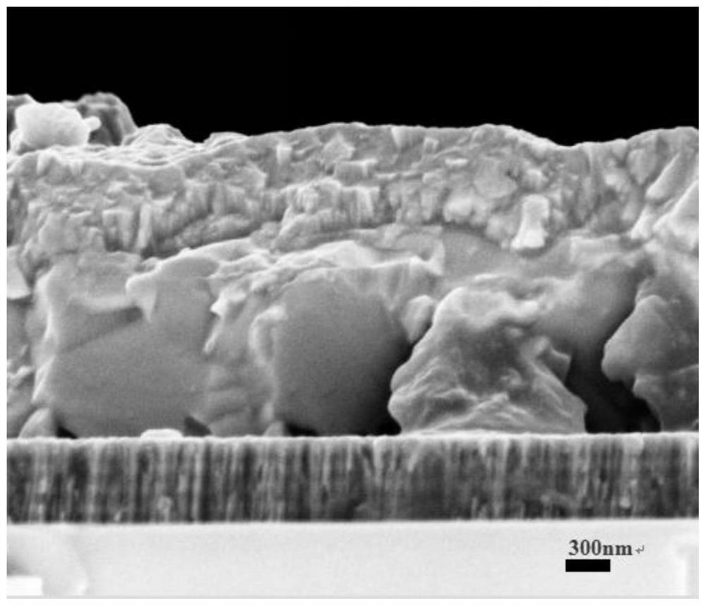
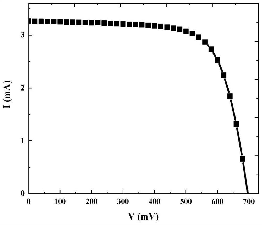
[0052] A first carrier transport layer with a thickness of 800nm and made of Mo was grown on a clean glass substrate by DC magnetron sputtering; a thickness of 1.7 μm was grown on the surface of the first carrier transport layer by a three-step co-evaporation method , the material is CuIn 0.6 Ga 0.4 Se 2 p-type optical absorption layer; grow a 120nm buffer layer made of n-type CdS by chemical water bath deposition on the p-type optical absorber layer; grow a 370nm thick buffer layer made of ZnMgO by radio frequency magnetron sputtering on the buffer layer N-type window layer; grown on the n-type window layer by radio frequency magnetron sputtering with a thickness of 50nm and made of BaTiO 3 The n-type ferroelectric film layer; on the ferroelectric film layer, a second carrier transport layer with a thickness of 690nm and made of aluminum-doped zinc oxide is grown by radio frequency sputtering; on the second carrier transport layer, the radio frequency magnetic A metal gr...
Embodiment 2
[0056] A first carrier transport layer with a thickness of 769.2 nm and made of Mo was grown on a clean glass substrate by DC magnetron sputtering; a thickness of 2.27 nm was grown on the surface of the first carrier transport layer by a three-step co-evaporation method. μm, material is CuIn 0.5 Ga 0.5 Se 2 p-type optical absorption layer; grow a 120nm buffer layer made of n-type CdS by chemical water bath deposition on the p-type optical absorber layer; grow a 370nm thick buffer layer made of ZnMgO by radio frequency magnetron sputtering on the buffer layer n-type window layer; grown on the n-type window layer by radio frequency magnetron sputtering with a thickness of 48nm and made of BaTiO 3 The n-type ferroelectric film layer; on the ferroelectric film layer, a second carrier transport layer with a thickness of 700nm and made of aluminum-doped zinc oxide is grown by radio frequency sputtering; on the second carrier transport layer, the radio frequency magnetic A metal g...
PUM
| Property | Measurement | Unit |
|---|---|---|
| thickness | aaaaa | aaaaa |
| thickness | aaaaa | aaaaa |
| thickness | aaaaa | aaaaa |
Abstract
Description
Claims
Application Information
 - R&D
- Intellectual Property
- Life Sciences
- Materials
- Tech Scout
- Unparalleled Data Quality
- Higher Quality Content
- 60% Fewer Hallucinations
Browse by: Latest US Patents, China's latest patents, Technical Efficacy Thesaurus, Application Domain, Technology Topic, Popular Technical Reports.
© 2025 PatSnap. All rights reserved.Legal|Privacy policy|Modern Slavery Act Transparency Statement|Sitemap|About US| Contact US: help@patsnap.com


