Chip structure and size conversion accelerator thereof

An accelerator and size technology, applied in the field of image processing, to achieve the effect of accelerating computing, reducing time consumption, and reducing data reading and writing steps

Pending Publication Date: 2022-04-12
SHANGHAI WESTWELL INFORMATION & TECH CO LTD
View PDF2 Cites 0 Cited by
  • Summary
  • Abstract
  • Description
  • Claims
  • Application Information

AI Technical Summary

Problems solved by technology

[0004] It can be seen that the current acceleration improvement of the bilinear interpolation algorithm mainly lies in the improvement of the algorithm and the hardware implementation of the size transformation, and neither considers how to realize the calculation of the size transformation from the direction of hardware reading and writing and caching of the bilinear interpolation algorithm. accelerate

Method used


Image

  • Chip structure and size conversion accelerator thereof
  • Chip structure and size conversion accelerator thereof
  • Chip structure and size conversion accelerator thereof

Examples


Embodiment Construction

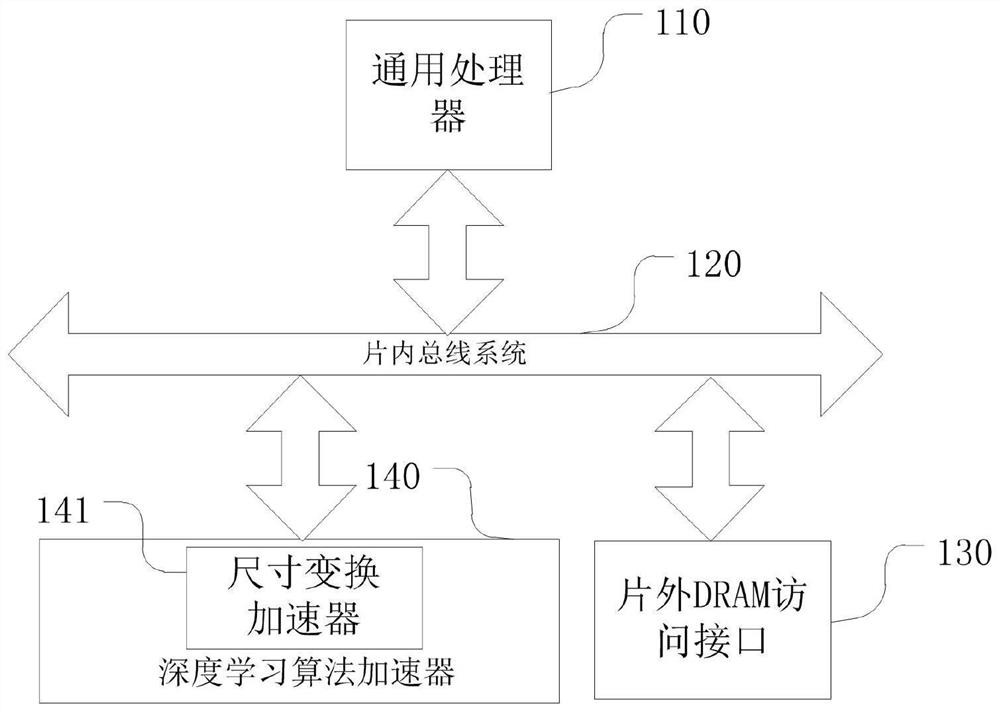
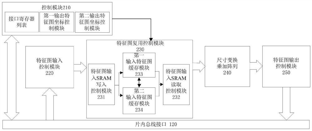
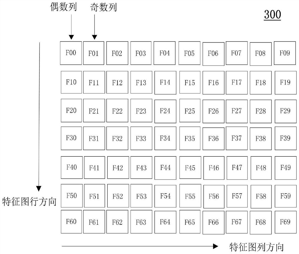
[0048] Example embodiments will now be described more fully with reference to the accompanying drawings. Example embodiments may, however, be embodied in many forms and should not be construed as limited to the examples set forth herein; rather, these embodiments are provided so that this disclosure will be thorough and complete and will fully convey the concept of example embodiments to those skilled in the art. The described features, structures, or characteristics may be combined in any suitable manner in one or more embodiments.

[0049] Furthermore, the drawings are merely schematic illustrations of the present disclosure and are not necessarily drawn to scale. The same reference numerals in the drawings denote the same or similar parts, and thus repeated descriptions thereof will be omitted. Some of the block diagrams shown in the drawings are functional entities and do not necessarily correspond to physically or logically separate entities. These functional entities ma...


PUM


Abstract

The invention provides a chip structure and a size conversion accelerator thereof. The size transformation accelerator includes a control module including an interface register list including a first register and a second register, and an output feature map coordinate control module to traverse coordinates of an output feature map, generating calculation parameters of size transformation based on an interface register list according to the coordinates of the output feature map; the feature map input control module is used for being connected with an on-chip bus; the feature map multiplexing control module is used for caching the image data of the input feature map and controlling writing and reading of the cached image data of the input feature map; the size transformation multiply-add array is used for transforming the image data of the input feature map into the image data of the output feature map according to the calculation parameters of size transformation in an assembly line mode; and the feature map output control module is used for being connected with an on-chip bus. According to the invention, size transformation acceleration is realized.

Description

technical field [0001] The invention relates to the field of image processing, in particular to a chip structure and a size conversion accelerator thereof. Background technique [0002] In the field of image processing, especially the deep learning network model of images, it is usually necessary to perform size transformation and size scaling on the input image. Therefore, size transformation operators are widely used in various deep learning algorithms. [0003] The commonly used algorithm for size transformation is bilinear interpolation algorithm. There are currently some accelerated calculation methods for the bilinear interpolation algorithm. Such as the announcement number CN104869284A, the name is a high-efficiency FPGA (Field-Programmable Gate Array, field-programmable gate array) of a bilinear interpolation amplification algorithm, the implementation method and device, which mainly pass two consecutive output pixels before and after, A set of calculation weights...

Claims


Application Information

Patent Timeline
IPC IPC(8): G06F12/0811G06F9/50
Inventor 谭黎敏宋捷桑迟
Owner SHANGHAI WESTWELL INFORMATION & TECH CO LTD
Why Eureka
Try Eureka