Automatic chip detection method and device

An automated detection and chip technology, applied in the field of detection, can solve the problems of high labor and man-hours, inability to quickly obtain the detection data of a single chip to be tested, secondary pollution, etc., to achieve accurate sorting and classification results, and improve detection and testing efficiency. , the effect of saving labor costs

Active Publication Date: 2022-04-08
ZHENGZHOU XINDA JIEAN INFORMATION TECH
View PDF7 Cites 0 Cited by
  • Summary
  • Abstract
  • Description
  • Claims
  • Application Information

AI Technical Summary

Problems solved by technology

[0002] The domestic semiconductor industry started late, and the appearance inspection and performance testing of chip products are usually performed manually, which requires a lot of manpower and man-hours, and it is easy to cause secondary pollution and damage during the inspection.
Moreover, the appearance inspection and performance test of the chip are usually two independent lines, and it is difficult to realize the correlation and fusion of the inspection data of the two.
Therefore, with the traditional chip detection method, even after all the chip detection processes are completed, it is impossible to quickly obtain the overall detection data of a single chip to be inspected, and it is impossible to accurately classify the chips to be inspected

Method used


Image

  • Automatic chip detection method and device
  • Automatic chip detection method and device

Examples


Embodiment Construction

[0037] In order to understand the above-mentioned purpose, features and advantages of the present invention more clearly, the present invention will be further described in detail below in conjunction with the accompanying drawings and specific embodiments. It should be noted that, in the case of no conflict, the embodiments of the present application and the features in the embodiments can be combined with each other.

[0038] In the following description, many specific details are set forth in order to fully understand the present invention. However, the present invention can also be implemented in other ways different from those described here. Therefore, the protection scope of the present invention is not limited by the specific details disclosed below. EXAMPLE LIMITATIONS.

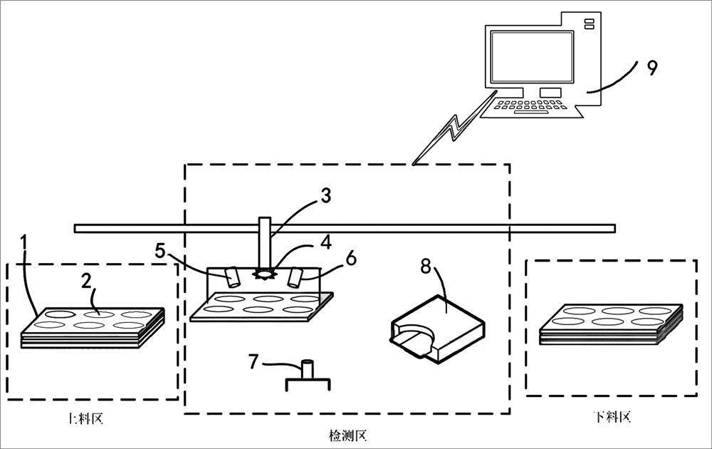
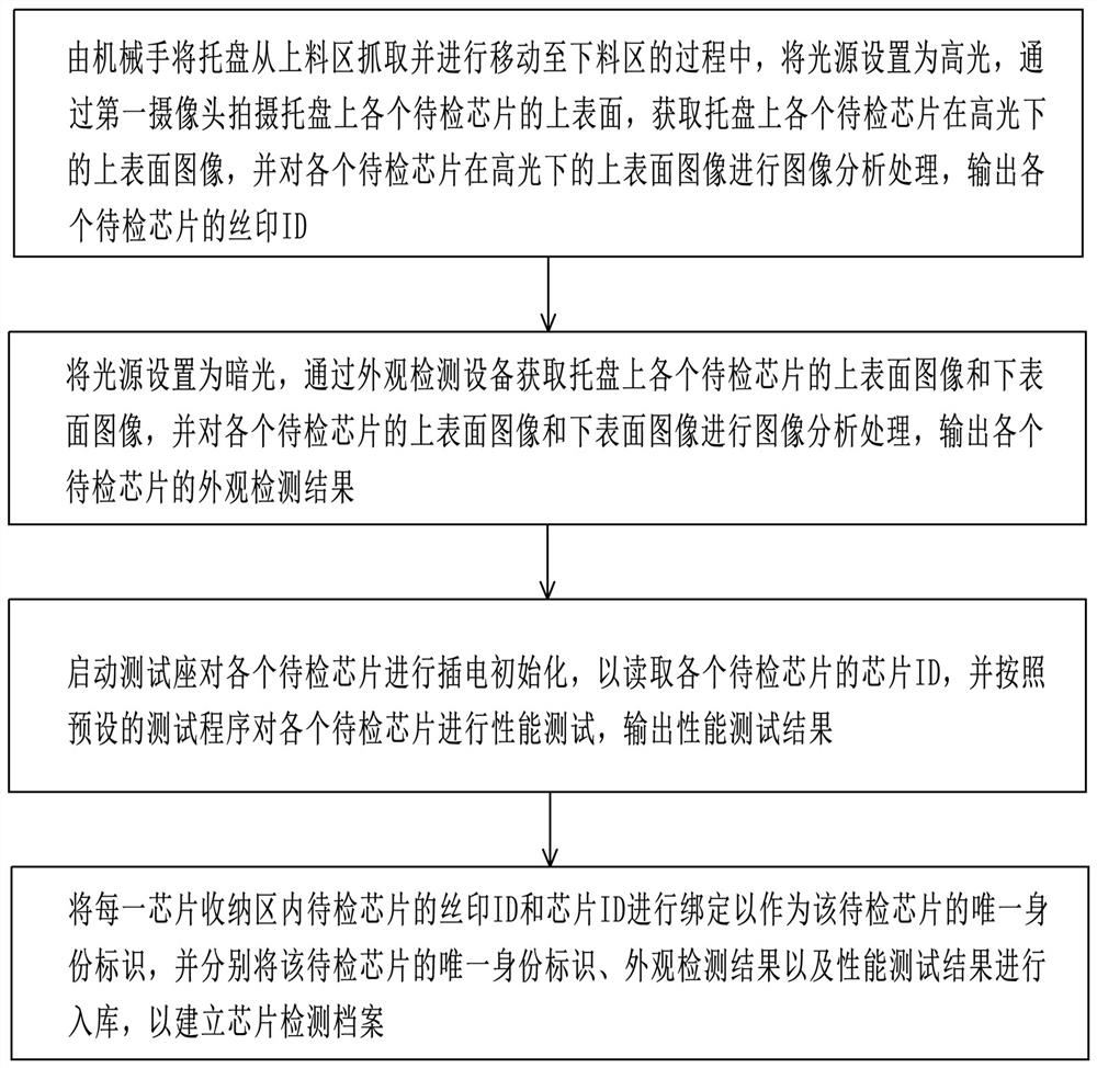
[0039] Such as figure 1 As shown, the present invention provides an automatic chip detection device, including: a tray, a manipulator, a light source, a first camera, appearance detection equipment,...


PUM


Abstract

The invention provides an automatic chip detection method and device, and the method comprises the steps: carrying out the silk-screen ID detection, appearance detection and performance detection in a process that a manipulator moves a tray from a feeding region to a discharging region; the method comprises the following steps: obtaining a screen printing ID through screen printing ID detection, and obtaining a chip ID during a performance test; then the silk-screen ID and the chip ID are combined to lock a specific chip, that is, the bound silk-screen ID and chip ID can be used as the unique identity of the chip, so that the appearance detection result and the performance test result of the chip can be integrated based on the unique identity of the chip; a user or a detection manager can conveniently and quickly know the overall condition of a specific chip, and the classification result is more accurate.

Description

technical field [0001] The invention relates to the technical field of detection, in particular to a chip automatic detection method and device. Background technique [0002] The domestic semiconductor industry started relatively late, and the appearance inspection and performance testing of chip products are usually performed manually, which requires a lot of manpower and man-hours, and is likely to cause secondary pollution and damage during inspection. Moreover, the appearance inspection and performance test of the chip are usually two independent lines, and it is difficult to realize the correlation and fusion of the inspection data of the two. Therefore, with the traditional chip detection method, even after the entire chip detection process is completed, it is impossible to quickly obtain the overall detection data of a single chip to be inspected, and it is impossible to accurately classify the chips to be inspected. Contents of the invention [0003] Based on the ...

Claims


Application Information

Patent Timeline
Patent Type & Authority Applications(China)
IPC IPC(8): B07C5/34B07C5/36B07C5/02
Inventor 刘熙胖王凯霖彭金辉李鑫
Owner ZHENGZHOU XINDA JIEAN INFORMATION TECH
Why Eureka
Try Eureka