Semiconductor structure and forming method thereof

A technology of semiconductor and channel structure, applied in the direction of semiconductor devices, semiconductor/solid-state device manufacturing, semiconductor/solid-state device components, etc., to reduce damage, improve uniformity, and reduce process difficulty

Pending Publication Date: 2022-03-29
SEMICON MFG INT (SHANGHAI) CORP +1
View PDF0 Cites 0 Cited by
  • Summary
  • Abstract
  • Description
  • Claims
  • Application Information

AI Technical Summary

Problems solved by technology

However, forming conductive plugs (Via-BPR) for electrically connecting buried power rails presents a major challenge

Method used


Image

  • Semiconductor structure and forming method thereof
  • Semiconductor structure and forming method thereof
  • Semiconductor structure and forming method thereof

Examples


Embodiment Construction

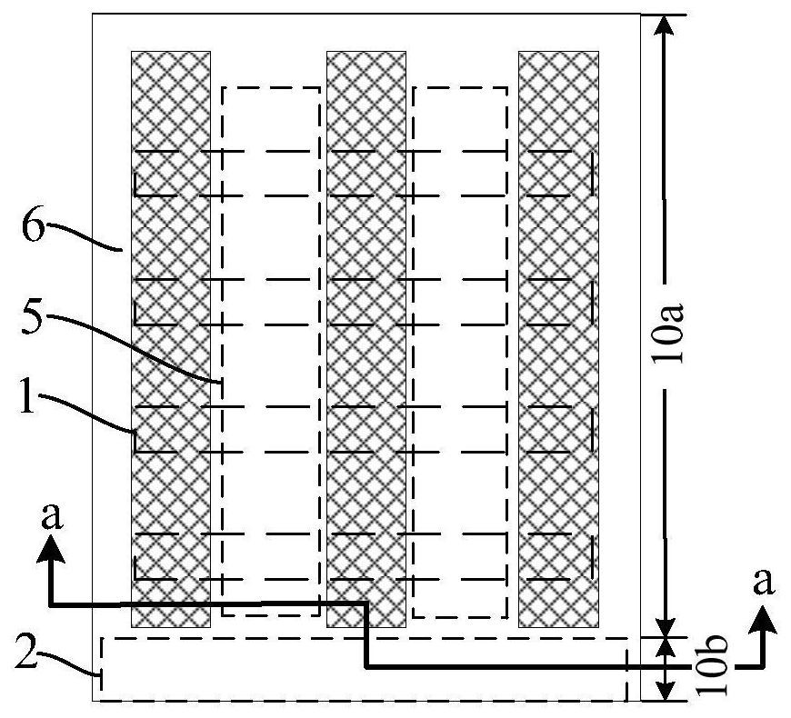
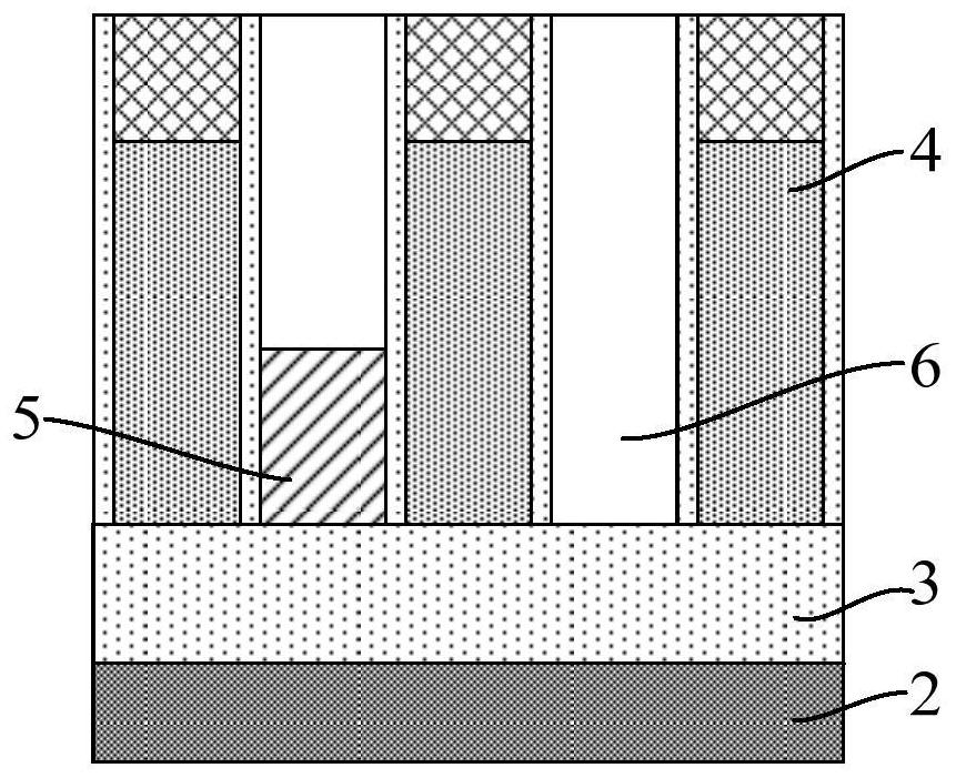
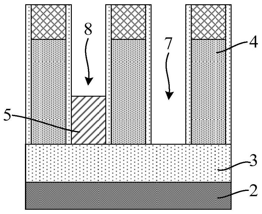
[0014] It can be seen from the background art that currently, forming a conductive plug (Via-BPR) for connecting buried power rails is a big challenge. The reason why forming a conductive plug (Via-BPR) is relatively challenging is now analyzed in combination with a method for forming a semiconductor structure. Figure 1 to Figure 5 It is a structural schematic diagram corresponding to each step in a method for forming a semiconductor structure.

[0015] refer to figure 1 with figure 2 , figure 1 for top view, figure 2 yes figure 1 A cross-sectional view along the aa direction provides a substrate (not shown), including a device region 10a and a power rail region 10b. A discrete channel structure 1 is formed on the substrate of the device region 10a, and a discrete channel structure 1 is formed on the substrate of the power rail region 10b. There are power track lines 2, the extension direction of the power track lines 2 is parallel to the extension direction of the c...


PUM


Abstract

The invention discloses a semiconductor structure and a forming method thereof. The forming method comprises the following steps: providing a substrate, a channel structure, a power supply track line, a gate structure, a source-drain doped region and an interlayer dielectric layer; forming conductive through holes penetrating through the interlayer dielectric layer located on part of the power supply track lines, wherein the conductive through holes comprise bottom through holes and top through holes located on the bottom through holes; forming a bottom plug in contact with the power supply track line in the bottom through hole; forming a filling dielectric layer for filling the top through hole on the bottom plug; etching the interlayer dielectric layer and the filling dielectric layer to form an interconnection groove penetrating through the interlayer dielectric layer at the top of the source-drain doped region, and exposing the top through hole; the top through hole and the interconnection groove are filled, a top plug which is located in the top through hole and makes contact with the bottom plug and a source-drain interconnection layer which is located in the interconnection groove and makes contact with the source-drain doped region are formed, and the top plug and the bottom plug form a conductive plug. According to the embodiment of the invention, the process window for forming the Via-BPR can be increased.

Description

technical field [0001] Embodiments of the present invention relate to the field of semiconductor manufacturing, and in particular, to a semiconductor structure and a method for forming the same. Background technique [0002] Logic chips are made up of standard cells. The size of the standard cell depends on the metal pitch, the height of the standard cell, the polysilicon pitch, and whether it is a single diffusion block (SDB) or a double diffusion block (DDB). Chip scaling has been driven by metal pitch (MP) and polysilicon pitch (PP) scaling for many years, but MP scaling is challenged by lithographic process limits and increased resistance. And due to device issues, polysilicon pitch scaling has slowed down. The introduction of Design Process Co-Optimization (DTCO) has made compressing standard cell heights the primary scaling option. As the cell height gradually shrinks, the number of fins for a single device per cell also gradually decreases, which will also result i...

Claims


Application Information

Patent Timeline
Patent Type & Authority Applications(China)
IPC IPC(8): H01L21/768H01L23/48
CPCH01L21/76805H01L23/481
Inventor 呼翔
Owner SEMICON MFG INT (SHANGHAI) CORP
Why Eureka
Try Eureka