Manufacturing method of alignment mark of photoetching machine and wafer

An alignment mark and manufacturing method technology, applied in the semiconductor field, can solve the problems of corrosion resolution, poor overlay accuracy, product rework, etc., and achieve the effect of improving yield and ensuring accuracy

Pending Publication Date: 2022-03-25
北海惠科半导体科技有限公司
View PDF16 Cites 1 Cited by
  • Summary
  • Abstract
  • Description
  • Claims
  • Application Information

AI Technical Summary

Problems solved by technology

The current wafer semiconductor products need three photolithography, the first photolithography is to make two alignment marks: the first mark and the second mark, the second photolithography is to engrave the second mark with the third mark sleeve, and the second photolithography The third lithography is to engrave the first mark with the fourth mark sleeve, because the second lithography is separated between the third lithography and the first lithography, so that the first mark made during the first lithography It is easy to be corroded by oxidant, which makes the resolution worse, making the signal worse and difficult to identify, resulting in poor overlay accuracy during the third photolithography, resulting in product rework or scrap

Method used


Image

  • Manufacturing method of alignment mark of photoetching machine and wafer
  • Manufacturing method of alignment mark of photoetching machine and wafer
  • Manufacturing method of alignment mark of photoetching machine and wafer

Examples


Embodiment Construction

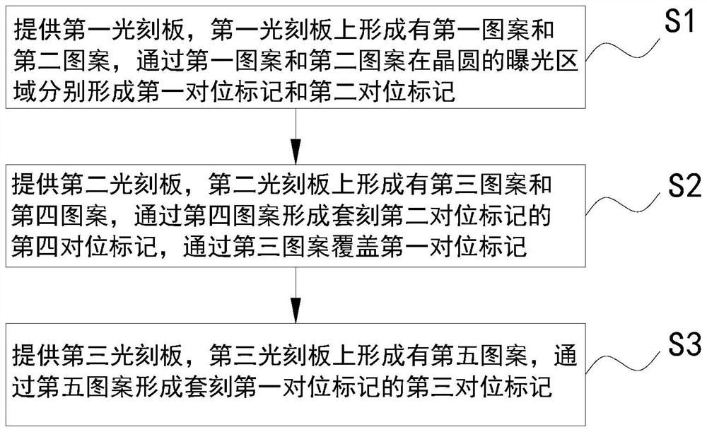
[0032] In order to make the purposes, technical solutions and advantages of the embodiments of the present application clearer, the technical solutions in the embodiments of the present application will be clearly and completely described below in conjunction with the drawings in the embodiments of the present application. Obviously, the described embodiments It is a part of the embodiments of this application, but not all of them. Based on the embodiments in the present application, all other embodiments obtained by persons of ordinary skill in the art without making creative efforts belong to the protection scope of the present application.

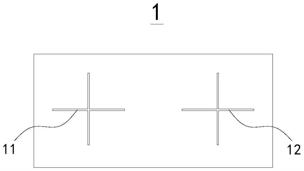
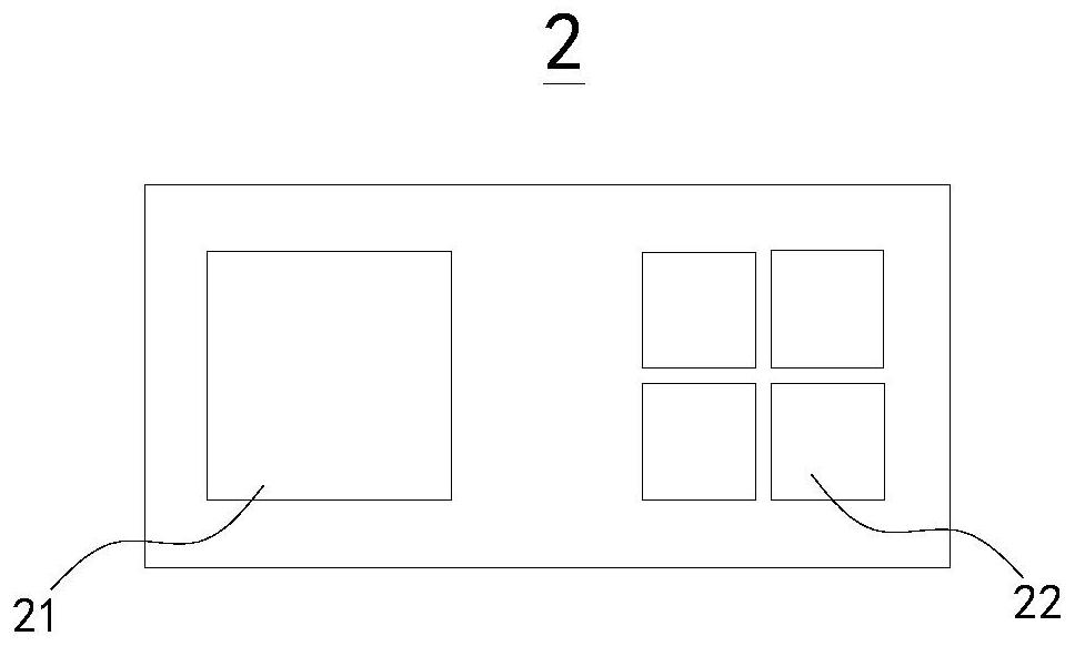
[0033] Such as figure 1 and 8 As shown, the embodiment of the present application provides a method for manufacturing an alignment mark of a lithography machine, including:

[0034] S1. Provide a first photoresist plate 1, on which a first pattern 11 and a second pattern 12 are formed, and the first alignment is formed in the exposure...


PUM

PropertyMeasurementUnit
lengthaaaaaaaaaa
widthaaaaaaaaaa
widthaaaaaaaaaa

Abstract

The invention relates to the technical field of semiconductors, in particular to a photoetching machine alignment mark manufacturing method and a wafer, the photoetching machine alignment mark manufacturing method comprises the following steps: providing a first photoetching plate, forming a first pattern and a second pattern on the first photoetching plate, respectively forming a first alignment mark and a second alignment mark in the exposure area of the wafer through the first pattern and the second pattern; providing a second photoetching plate, forming a third pattern and a fourth pattern on the second photoetching plate, forming a fourth alignment mark on which the second alignment mark is overlaid through the fourth pattern, and covering the first alignment mark through the third pattern; and providing a third photoetching plate, forming a fifth pattern on the third photoetching plate, and forming a third alignment mark on which the first alignment mark is overlaid through the fifth pattern. According to the manufacturing method of the alignment mark of the photoetching machine, the alignment precision and the yield of the alignment mark can be improved.

Description

technical field [0001] The present application relates to the technical field of semiconductors, in particular to a method for manufacturing an alignment mark of a photolithography machine and a wafer. Background technique [0002] Photolithography is a key process for precision pattern production in the semiconductor industry, because the pattern structure is micron or submicron level, and pattern overlay between different layers is required. The current wafer semiconductor products need three photolithography, the first photolithography is to make two alignment marks: the first mark and the second mark, the second photolithography is to engrave the second mark with the third mark sleeve, and the second photolithography The third lithography is to engrave the first mark with the fourth mark sleeve, because the second lithography is separated between the third lithography and the first lithography, so that the first mark made during the first lithography It is easy to be co...

Claims


Application Information

Patent Timeline
Patent Type & Authority Applications(China)
IPC IPC(8): G03F9/00H01L21/66
CPCG03F9/7073G03F9/7076G03F9/708H01L22/20
Inventor 王占伟王国峰
Owner 北海惠科半导体科技有限公司
Why Eureka
Try Eureka