Wafer test equipment

A technology of wafer testing and equipment, applied in the field of wafer testing equipment, can solve problems such as inability to realize continuous operation, affect test efficiency, and affect test results, so as to avoid clamping damage, protect wafers, and ensure accuracy Effect

Active Publication Date: 2022-03-25
江苏威森美微电子有限公司
View PDF17 Cites 1 Cited by
  • Summary
  • Abstract
  • Description
  • Claims
  • Application Information

AI Technical Summary

Problems solved by technology

[0007] In order to make up for the deficiencies of the existing technology and solve the problem that during the inspection process, due to the reciprocal adjustment of the wafer positioning, it will cause wear and affect the quality of the wafer. During the feeding process, the stability is not good, which affects the test results. After the inspection is completed , can not realize the continuous operation, the problem of affecting the efficiency of testing, a kind of wafer testing equipment proposed by the present invention

Method used


Image

  • Wafer test equipment
  • Wafer test equipment
  • Wafer test equipment

Examples


Embodiment

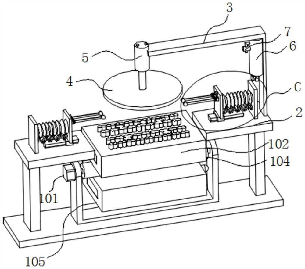
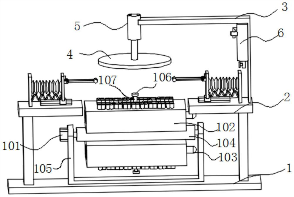
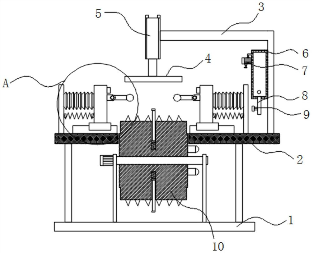
[0033] Such as Figure 1 to Figure 7As shown, a wafer testing device according to the present invention includes a base 1, a mounting plate 2, a mounting frame 3, a rubber backing plate 4, a cylinder 5, an air storage tank 6, an air pump 7, an air release pipe 8, and a solenoid valve 9 , overturning structure 10, overturning motor 101, probe plate 102, warning light 103, rotating shaft 104, support frame 105, gasket 106, movable rod 107, first conductive plate 108, second conductive plate 109, limit cap 110 , the first spring 111, the guide rail 201, the slide button 202, the second spring 203, the baffle plate 204, the air bag 205, the trigger button 206, the rubber ball 207, the swing seat 208, the supporting plate 209, and the mounting plate 2 is erected above the base 1, A support frame 105 is installed on the base 1, and a rotating shaft 104 is mounted on the support frame 105 through a bearing. A turning motor 101 is installed on one side of the supporting frame 105, and...


PUM


Abstract

The invention belongs to the technical field of semiconductor processing, and particularly relates to wafer testing equipment which comprises a base and a mounting plate, the mounting plate is erected above the base, a rubber ball is in contact with a wafer, wafer lifting and air pump operation are achieved, air inlet of an air storage tank is achieved, air inlet of an air bag is achieved through a guide pipe, and after air inlet of the air bag, the air inlet of the air bag is closed. A sliding buckle is arranged at the bottom of the supporting plate, in the pushing process, the sliding buckle slides along a guide rail, center positioning of a wafer is achieved, after clamping, the two sides of the wafer make contact with a trigger button, extrusion of the trigger button is achieved, an electric signal is connected and received by a PLC processor, and air inlet operation is stopped; flexible extrusion and accurate positioning can be realized, clamping damage of a wafer is avoided, the feeding accuracy is ensured, abrasion under conventional calibration actions is reduced, the wafer is better protected, overturning discharging is realized, feeding is synchronously realized, continuous operation can be realized, and the detection efficiency is improved.

Description

technical field [0001] The invention belongs to the technical field of semiconductor processing, in particular to wafer testing equipment. Background technique [0002] Semiconductor refers to a material whose conductivity is between that of a conductor and an insulator at room temperature. Semiconductors are widely used in radios, televisions, and temperature measurement. For example, diodes are devices made of semiconductors. Semiconductors refer to a kind of electrical conductivity that can be controlled. , ranging from materials between insulators to conductors, whether from the perspective of technology or economic development, the importance of semiconductors is huge, most of today's electronic products, such as computers, mobile phones or digital recorders The core units are all closely related to semiconductors. Common semiconductor materials include silicon, germanium, gallium arsenide, etc., and silicon is the most influential one in commercial applications among v...

Claims


Application Information

Patent Timeline
Patent Type & Authority Applications(China)
IPC IPC(8): G01R31/26
CPCG01R31/26
Inventor 陈贵林谭进柳天勇
Owner 江苏威森美微电子有限公司
Why Eureka
Try Eureka