
Quickly-opened floating island device and manufacturing method thereof

A floating island and fast technology, applied in semiconductor/solid-state device manufacturing, semiconductor devices, electrical components, etc., can solve the problems of belt bending, hindering the flow of electronic carriers, and unable to restore the conduction ability, so as to increase the current conduction capacity, the effect of reducing width

Active Publication Date: 2022-03-22
ZHEJIANG UNIV
View PDF16 Cites 2 Cited by
  • Summary
  • Abstract
  • Description
  • Claims
  • Application Information

AI Technical Summary

Problems solved by technology

[0003] Breakdown voltage is an important indicator of semiconductor power devices, which indicates the maximum voltage that the device can withstand. Floating island device (or floating junction device) refers to a special power device, in which there is Directly connected, and the doping type is opposite to that of the drift region, at the moment when the floating island device doped as N-type in the drift region changes from the blocking state to the conducting state, due to the P-type doping region inside the drift region and the electrode Without a direct connection, hole carriers cannot enter the P-type doped region, resulting in negative charges remaining in the P-type doped region, while a large number of positive charges are attracted to the N-type drift region, occupying the space charge. The full drift region causes the energy band to bend, thereby hindering the flow of electron carriers, that is, the floating island device with a floating doped region in the drift region cannot complete the conduction recovery at low voltage
In this case, only when the bias voltage is large enough, the charge can conduct through the drift region, but when the bias voltage is low, there is a problem that the conduction ability cannot be restored

Method used


Image

  • Quickly-opened floating island device and manufacturing method thereof
  • Quickly-opened floating island device and manufacturing method thereof
  • Quickly-opened floating island device and manufacturing method thereof

Examples


Embodiment 1

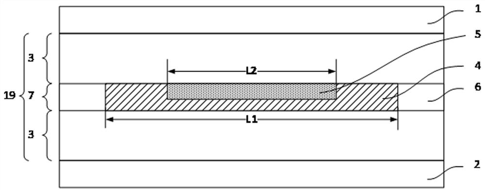
[0062] At the moment when the existing floating island device changes from the blocking state to the conducting state, since the P-type doped regions inside the drift region are not directly connected to the electrodes, the hole carriers near the anode cannot enter these P-type doped regions. In the P-type doped region, negative charges remain in the P-type doped region, and in the drift region, a large number of positive charges are attracted, occupying the N-type drift region in the form of space charges, causing energy band bending, and changing from a blocking state to a zero-biased state. When it is pressed, its energy band bends as shown in Figure 33, thereby hindering the flow of electron carriers, and the existing solution is to increase the voltage so that the charge can conduct electricity through the drift region, such as Figure 34 Shown is the energy band diagram when the voltage is increased to 692V.

[0063] As shown in Figure 1, in view of the above-mentioned p...

Embodiment 2

[0074] The floating island layer 7 in Fig. 1 can have multiple designs, as shown in Fig. 3, the position of the second doped region 5 relative to the first doped region 4 can be moved to the left, such as the position of the second doped region 5 The left edge stretches out to the left of the left edge of the first doped region 4, or the right edge of the second doped region 5 stretches out to the right of the right edge of the first doped region 4, at this time the second doping The length L2 of the portion of the region 5 located in the first doped region 4 is smaller than the length L1 of the first doped region 4 .

Embodiment 3

[0076] The floating island layer in Figure 1 can have various design schemes, as shown in Figure 4, the third doped region 6 can be set on one side of the first doped region 4, and the third doped region 6 can not be set on the other side .


PUM


Abstract

The invention relates to a quickly-opened floating island device and a manufacturing method thereof in the technical field of semiconductors, the quickly-opened floating island device comprises a surface layer, a bottom layer and a drift region, the drift region comprises a plurality of groups of substrate layers and a plurality of groups of floating island layers, one group of floating island layers is arranged between every two groups of substrate layers, or one group of substrate layers is arranged between every two groups of floating island layers, and the surface layer is arranged between the surface layer and the bottom layer. A heavily-doped inversion region is arranged in the floating island layer, so that the floating island device has the advantage of eliminating the obstruction of space charges to current, and the problem that the conduction capability of the floating island device with an opposite type of doping region in a drift region cannot be recovered under relatively low bias voltage is solved.

Description

technical field [0001] The invention relates to the technical field of semiconductors, in particular to a fast-turn-on floating island device and a manufacturing method thereof. Background technique [0002] In recent years, more and more attention has been paid to energy saving and emission reduction in the world, which puts forward higher requirements for loss control and efficiency improvement of large power electronic equipment. As an important part of power electronic equipment, semiconductor power devices have received extensive attention from the industry. . [0003] Breakdown voltage is an important indicator of semiconductor power devices, which indicates the maximum voltage that the device can withstand. Floating island device (or floating junction device) refers to a special power device, in which there is Directly connected, and the doping type is opposite to that of the drift region, at the moment when the floating island device doped as N-type in the drift reg...

Claims


Application Information

Patent Timeline
Patent Type & Authority Applications(China)
IPC IPC(8): H01L29/06H01L29/872H01L29/739H01L29/78H01L21/329H01L21/331H01L21/336
CPCH01L29/872H01L29/66143H01L29/66325H01L29/66477H01L29/7393H01L29/78H01L29/0684H01L29/7397H01L29/7813H01L29/0623H01L29/861H01L29/0619H01L29/66734H01L29/0688H01L29/8613
Inventor 盛况王策王珩宇任娜
Owner ZHEJIANG UNIV
Learn More