Chip chemical tinning processing technology

A technology of electroless tin plating and processing technology, applied in liquid chemical plating, metal material coating process, coating and other directions, which can solve the problems of residue, inability to ensure clean water, and the clamping end cannot be cleaned by clean water, etc. , to achieve good cleaning, improve stirring effect, and improve the effect of filtration efficiency

Pending Publication Date: 2022-03-22
深圳市宏达秋科技有限公司
View PDF0 Cites 0 Cited by
  • Summary
  • Abstract
  • Description
  • Claims
  • Application Information

AI Technical Summary

Problems solved by technology

[0003] At present, there are the following problems in the chemical tin plating process of chips: a. The tin plating solution will remain on the surface of the chip after being tinned by the chemical tin plating solution, so the chip needs to be cleaned with clean hot water immediately after the tin plating is completed to prevent There are spots and stains on the surface of the chip coating, and the chip is generally clamped by a clamp during cleaning so that it can be cleaned in clean water, which causes the problem that the contact part between the clamping end and the chip surface cannot be cleaned by clean water ; b. At the same time, the chip needs to ensure that the cleaning water is kept sufficiently clean during the cleaning process, and most of the existing methods are to regularly replace the cleaning water and clean the cleaning pool, which cannot ensure that the cleaning water in the cleaning pool is always kept clean , resulting in tin plating liquid impurities still remaining on the chip surface

Method used


Image

  • Chip chemical tinning processing technology
  • Chip chemical tinning processing technology
  • Chip chemical tinning processing technology

Examples


Embodiment Construction

[0037] Embodiments of the present invention will be described below with reference to the drawings. In the process, in order to ensure the clarity and convenience of illustration, we may exaggerate the width of the lines or the size of the constituent elements in the diagram.

[0038]In addition, the following terms are defined based on the functions in the present invention, and may be different according to the operator's intention or practice. Therefore, these terms are defined based on the entire content of this specification.

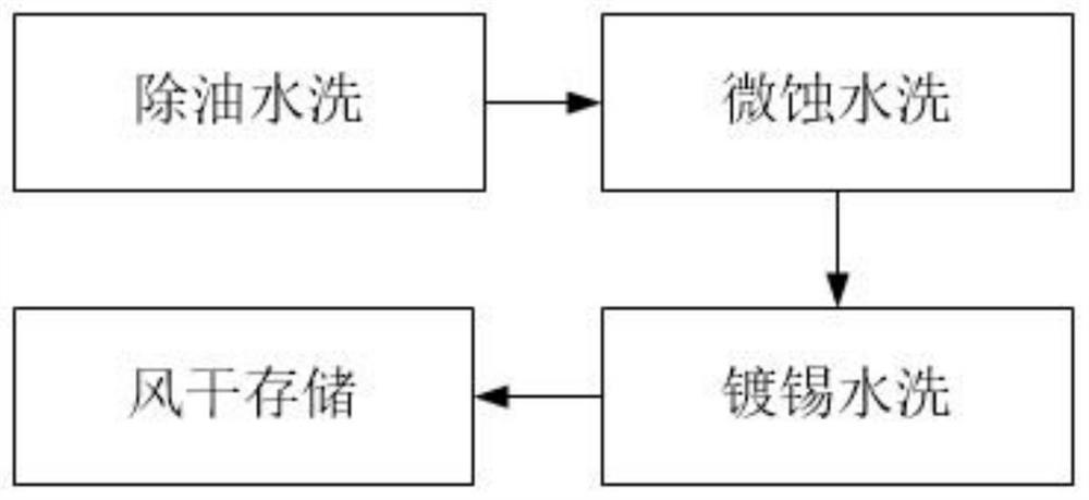
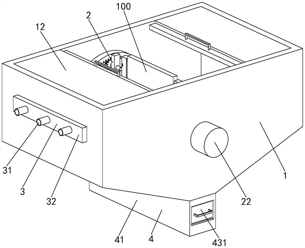
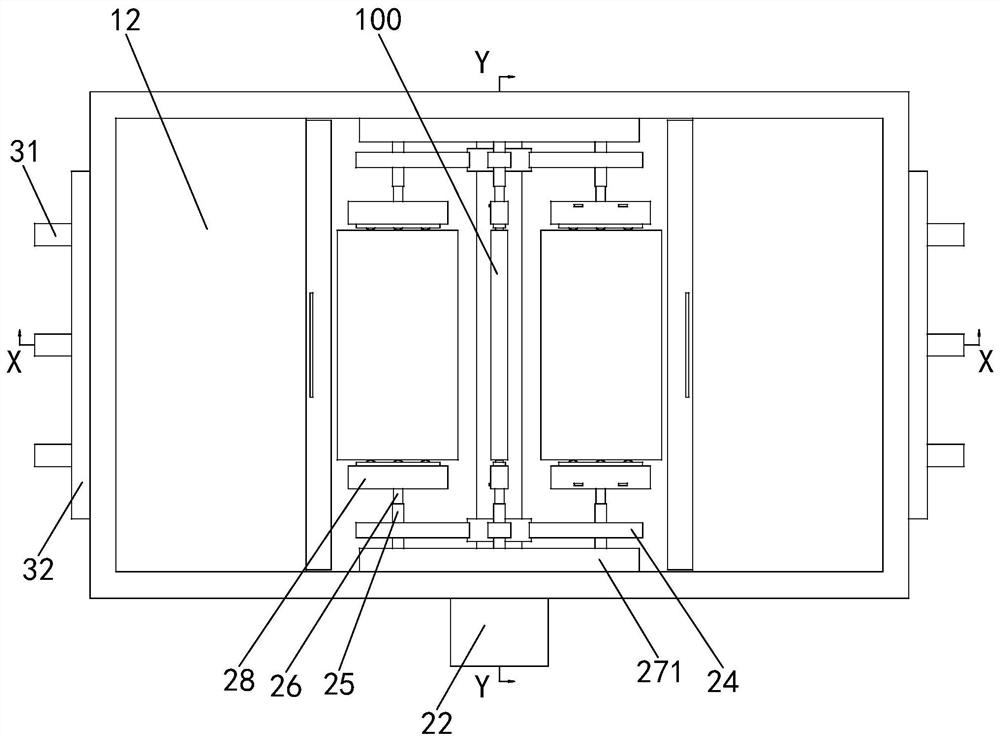
[0039] refer to Figure 1 to Figure 3 , a chip chemical tin plating processing technology, which uses chip chemical tin plating processing equipment, the equipment includes a washing frame 1, a washing device 2, a water inlet device 3 and a drainage device 4, and the specific method is as follows when using the above equipment operation: S1 , Degreasing and water washing: clean the grease and stains on the surface of the chip, so as not to affect...


PUM


Abstract

The invention relates to the technical field of chip tin plating processing, in particular to a chip chemical tin plating processing technology, chip chemical tin plating processing equipment is used, the equipment comprises a washing frame, a washing device, a water inlet device and a water drainage device, the washing frame is of a shell structure with an opening in the upper end, the washing device is arranged in the washing frame, and the water inlet device is arranged in the washing frame. Water inlet devices are arranged on the left and right sides of the washing frame, and a drainage device is arranged at the bottom of the washing frame. According to the chip cleaning device, the function of cleaning a plurality of chips at the same time can be achieved, meanwhile, it can be ensured that the surfaces of the chips can be cleaned by cleaning water, the cleaning water in the washing frame keeps flowing all the time through the water inlet device and the water drainage device, it is ensured that the cleaning water is kept clean enough all the time, and the surfaces of the chips are cleaned up.

Description

technical field [0001] The invention relates to the technical field of chip tin plating, in particular to a chip chemical tin plating process. Background technique [0002] Tin plating and its alloys are coatings with good solderability and certain corrosion resistance, and are widely used in electronic components and printed circuit boards. In addition to physical methods such as hot dipping and spraying, methods such as electroplating, immersion plating and chemical plating have been widely used in industry because of their simplicity. Electroless tin plating water can be used for chemical tin plating on the surface of copper alloys such as copper, brass, beryllium copper, etc. The tin plating is bright and silvery white, which can increase the weldability and decoration of copper without affecting the conductivity. It can be used in the electronics industry, furniture Utensils, food packaging, etc. The process of electroless tin plating mainly includes steps such as deg...

Claims


Application Information

Patent Timeline
IPC IPC(8): H01L21/02H01L21/67C23C18/31
CPCH01L21/02068H01L21/6704H01L21/67057C23C18/31C23C18/1689C23C18/1632C23C18/1642
Inventor 杨义华文明立
Owner 深圳市宏达秋科技有限公司
Why Eureka
Try Eureka