Double-excitation pressure memory device
A technology of memory device and pressure, applied in the measurement of the property force of piezoelectric resistance materials, digital memory information, instruments, etc., can solve the problems of signal attenuation, low energy conversion efficiency, large strain space and stress intensity, etc.
- Summary
- Abstract
- Description
- Claims
- Application Information
AI Technical Summary
Problems solved by technology
Method used
Image
Examples
Embodiment Construction
[0028] The specific implementation manners of the present invention will be further described below in conjunction with the accompanying drawings and technical solutions.
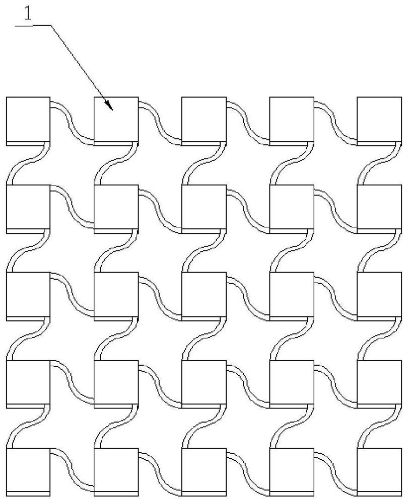
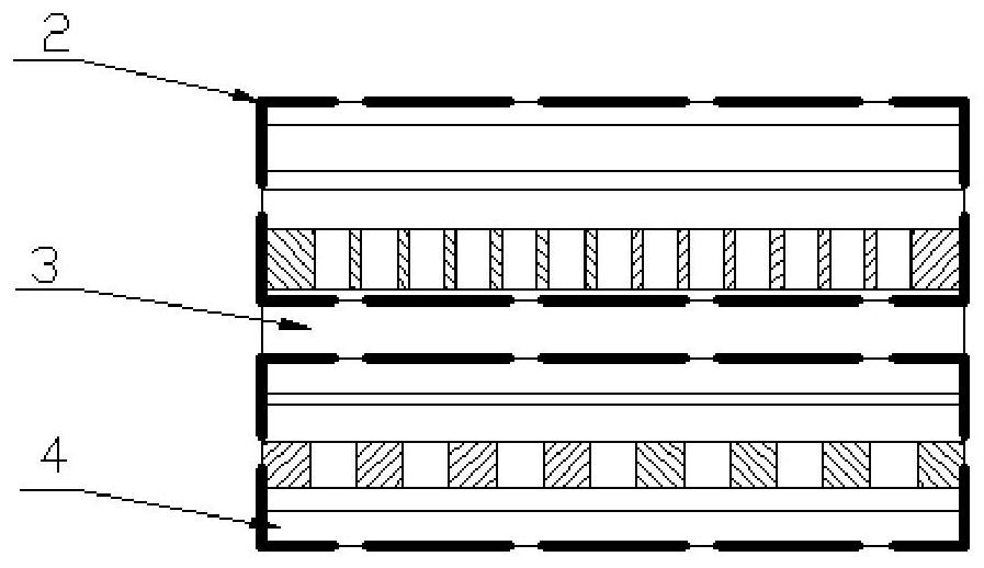
[0029] Figure 1(a), Figure 1(b) and figure 2 As shown, a kind of dual excitation pressure memory device of the present invention is formed DPM device matrix by DPM device 1; Composed of alternating arrangement, the piezoelectric memristor 4 is located at the bottom, the piezoelectric OLED2 is located at the top, and a PI (polyimide) insulating layer 3 is coated between the piezoelectric memristor and the piezoelectric OLED, and the piezoelectric memristor array The functional layer is covered by a piezoelectric OLED array.
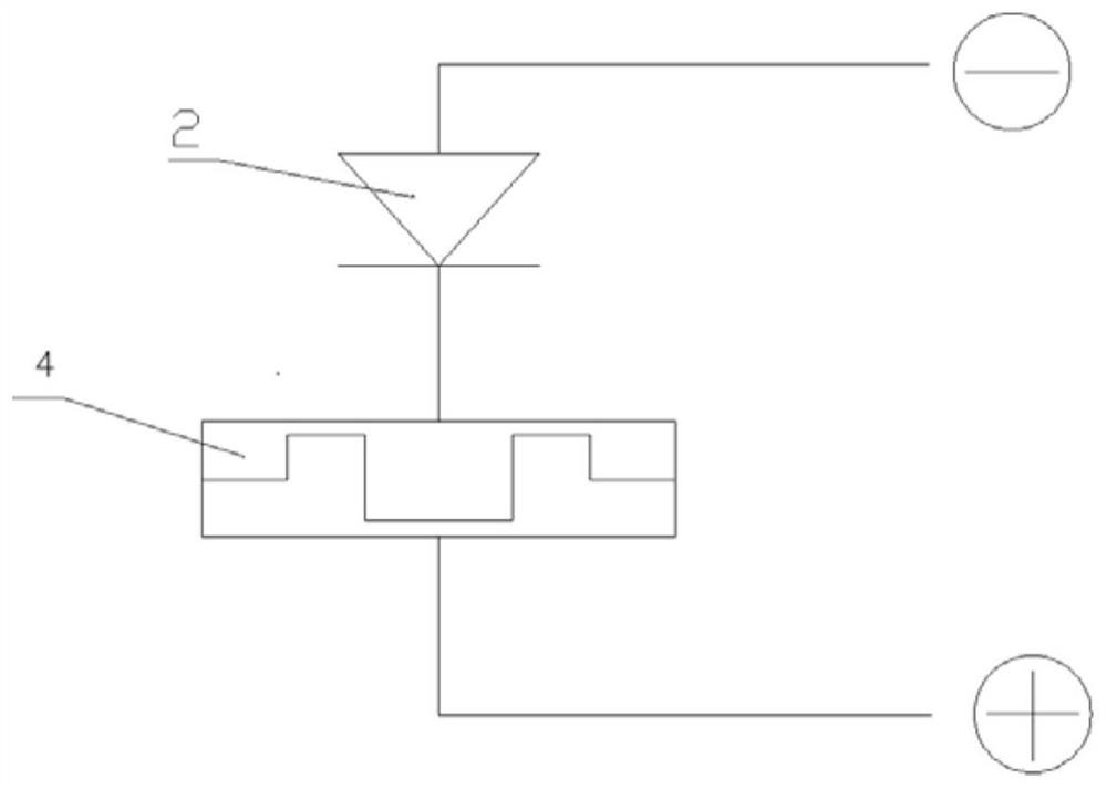
[0030] like image 3 As shown, the structure of the piezoelectric memristor is, from the bottom up, PET substrate 14, Cr / Ag layer 13 (Cr thickness is 4-6nm, Ag thickness is 45-55nm), PMMA layer 12 (thickness 1.8-2.1μm, ZnO embedded in PMMA, the same thickness), MoO x Layer 5 (thickn...
PUM
 Abstract
Description
Claims
Application Information
 - R&D
- Intellectual Property
- Life Sciences
- Materials
- Tech Scout
- Unparalleled Data Quality
- Higher Quality Content
- 60% Fewer Hallucinations
Browse by: Latest US Patents, China's latest patents, Technical Efficacy Thesaurus, Application Domain, Technology Topic, Popular Technical Reports.
© 2025 PatSnap. All rights reserved.Legal|Privacy policy|Modern Slavery Act Transparency Statement|Sitemap|About US| Contact US: help@patsnap.com


