Wafer laser coding method and wafer laser coding system

A laser beam and laser light source technology, applied in laser welding equipment, electrical components, circuits, etc., can solve the problems of code recognition difficulty, poor code effect, poor anti-counterfeiting, etc., and achieve good code position consistency and low cost , good anti-counterfeiting effect

Pending Publication Date: 2022-03-18
南光高科(厦门)激光科技有限公司
View PDF0 Cites 0 Cited by
  • Summary
  • Abstract
  • Description
  • Claims
  • Application Information

AI Technical Summary

Problems solved by technology

[0005] This application proposes a wafer laser coding method and a wafer laser coding system, aiming to solve the problems of poor precision, high cost, non-environmental protection, easy alteration, poor anti-counterfeiting, And the problems of poor coding effect and difficult code recognition make it improve accuracy, reduce cost, good environmental protection, code coding is not easy to fall off and alter, good anti-counterfeiting performance, good coding effect and easy identification

Method used


Image

  • Wafer laser coding method and wafer laser coding system
  • Wafer laser coding method and wafer laser coding system
  • Wafer laser coding method and wafer laser coding system

Examples


Embodiment 1

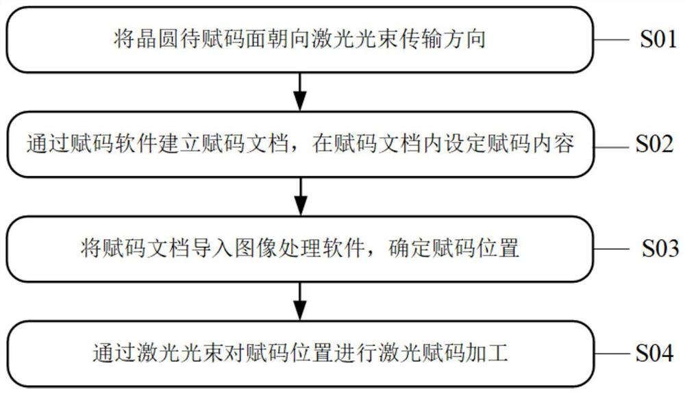
[0037] see figure 1 , a wafer laser coding method, comprising the following steps:

[0038] Step S01, facing the to-be-coded surface of the wafer 1 towards the transmission direction of the laser beam;

[0039] Step S02, using the coding software to create a coded file, and set the coded content in the coded file;

[0040] Step S03, import the coded document into the image processing software 2, and determine the coded position;

[0041] Step S04 , performing laser coding processing on the coding position by using a laser beam.

[0042] In some specific embodiments, after step S01 and before step S02, step S011 is set to adjust the size of the laser spot that the laser beam acts on the surface to be coded of the wafer 1;

[0043] In some specific embodiments, in step S011, by adjusting the distance between the laser light source of the laser beam and the surface to be coded of the wafer 1, the laser spot of the laser beam acting on the surface to be coded of the wafer 1 is ...

Embodiment 2

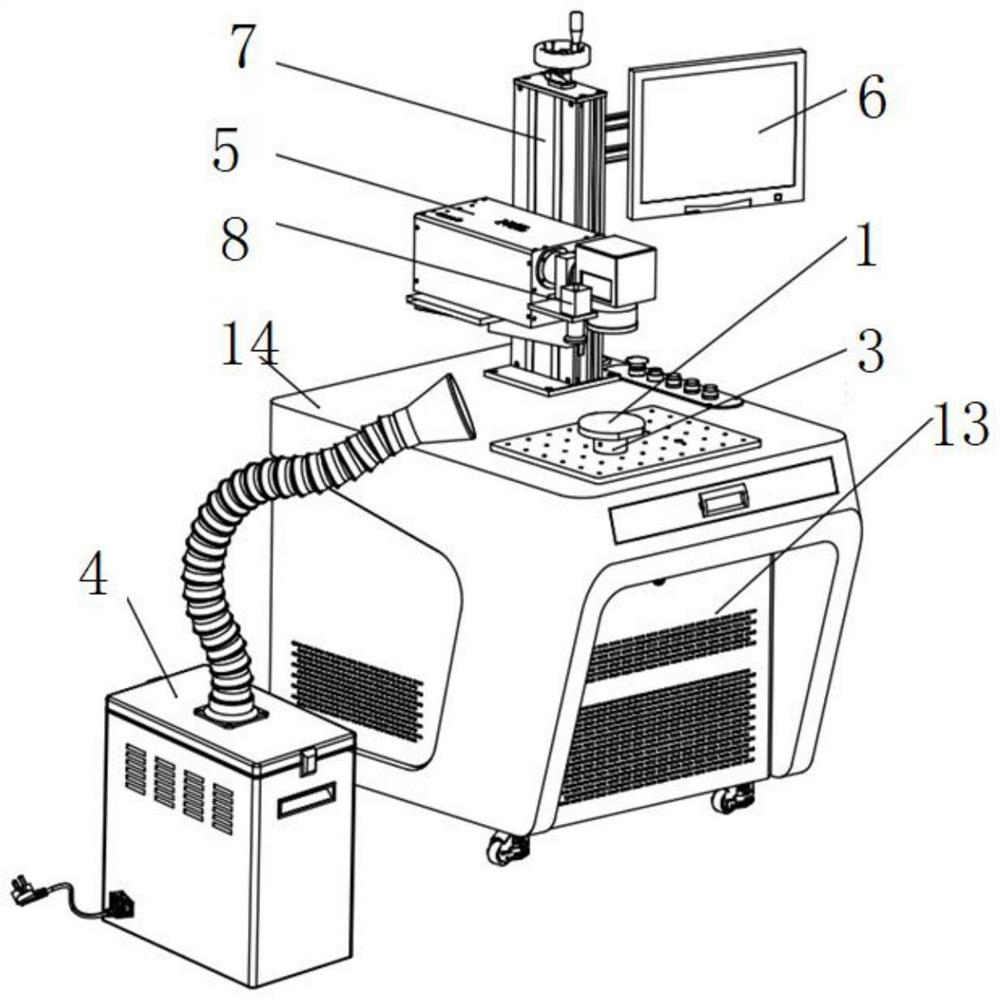
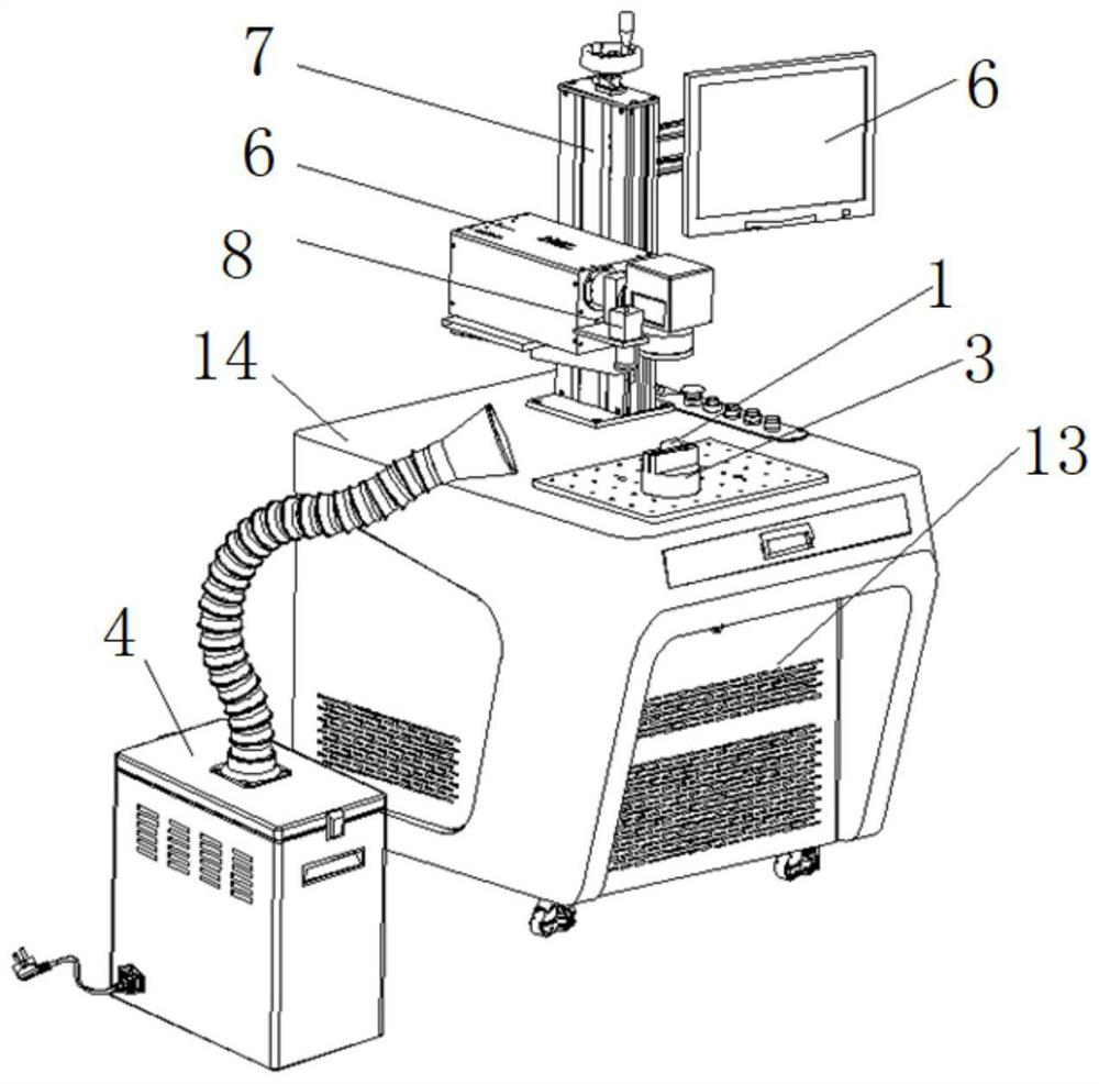
[0057] see figure 2 with image 3 , the present invention provides a wafer laser coding system for implementing the wafer laser coding method described in any one of Embodiment 1, the wafer laser coding system comprising:

[0058] The laser light source 5 is used to emit a laser beam for laser coding processing;

[0059] The industrial computer 6 is used to install coding software and image processing software 2. The coding software is used to control the filling method, filling distance, filling angle and laser parameters, and the image processing software 2 is used to determine the coding position.

[0060] In some specific embodiments, the laser light source 5 is installed on the distance adjustment device 7, and the distance adjustment device is used to adjust the distance between the laser light source 5 of the laser beam and the surface to be coded of the wafer 1, so as to realize the adjustment of the laser beam acting on The size of the laser spot on the surface of ...


PUM


Abstract

The invention discloses a wafer laser tagging method and a wafer laser tagging system. The wafer laser tagging method comprises the following steps: enabling a to-be-tagged surface of a wafer to face the transmission direction of a laser beam; establishing a tagging document through tagging software, and setting tagging contents in the tagging document; importing the tagging document into image processing software, and determining a tagging position; laser tagging processing is conducted on the tagging position through a laser beam; the processing process is free of consumables and pollution, the cost is lower, and the anti-counterfeiting property is better; a hyperfine mark is formed on the surface or inside the wafer under the action of a high-energy-density laser beam; non-contact machining is adopted, mechanical stress is avoided, and the product quality can be effectively improved; and positioning and code assigning can be achieved through machine vision, the alignment precision is high, the clamp can be placed at any angle within the machining plane range, the code assigning position consistency is good, and the production efficiency is greatly improved.

Description

technical field [0001] The present application relates to the technical field of laser coding, in particular to a wafer laser coding method and a wafer laser coding system. Background technique [0002] Wafers, for example, may be silicon wafers used to fabricate silicon semiconductor circuits, the starting material of which is silicon. High-purity polycrystalline silicon is dissolved and mixed with silicon crystal seeds, and then slowly pulled out to form cylindrical single crystal silicon. The silicon ingot is ground, polished, and sliced ​​to form a silicon wafer, that is, a wafer. [0003] Wafers generally have the characteristics of high hardness, high brittleness, and poor thermal conductivity. The wafer marking step is an indispensable step in the semiconductor manufacturing process, and its purpose is mainly to mark the ID (Identity) of the wafer, so as to facilitate the tracking of the wafer in the subsequent manufacturing, testing and packaging processes of the w...

Claims


Application Information

Patent Timeline
Patent Type & Authority Applications(China)
IPC IPC(8): B23K26/362B23K26/142B23K26/064B23K26/03B23K26/70H01L21/67
CPCB23K26/362B23K26/032B23K26/064B23K26/142B23K26/702H01L21/67282
Inventor 丘国雄贾富强陈银榕冯涣李巍伟叶泽群
Owner 南光高科(厦门)激光科技有限公司
Why Eureka
Try Eureka